When I first learned French in school, we were first introduced to the regular verbs. I was thinking: “Alright, this is pretty easy and makes sense. I just need to apply the rules and should be fine.” A month and a lot of irregular verbs later I was not fine, but very frustrated: Why were there so many exceptions to these rules? Why were there so many exceptions on the verbs I actually needed?
C++ can feel strangely reminiscent of that time when it comes to keywords affecting linkage and storage duration. I am specifically talking about:
static
extern
consteval
thread_local
volatile
constexpr
inline
const
constinit
We could interrogate these from various viewpoints, but here I will only look at how they modify to entity storage duration and linkage. A small disclaimer that this is a guideline based on my current state of knowledge. For specifics and edge-cases, please read the standard and run your own experiments on the compiler of your choice. In an attempt to keep this blog post shorter than the one on building a computer, I will glance over some details here and there (e.g., copy elision, move semantics and similar compiler optimizations) as well. If you find any mistakes, inaccuracies or have other comments, shoot me a message! Lastly, all things discussed here are using c++23 but mostly apply to earlier revisions too (but pay additional attention concerning pre C++17 inline and constexpr, constinit and consteval).
Now, because these keywords each depend on the context on how they are used I will structure the post bottom-up. We think about the possible effects there are and try to associate keywords and context to each effect. sMore concretely I structured this post as follows. First, some high-level background about how a C++ program is build. We then cover storage duration and subsequently linkage for variables before moving onto linkage of functions. I also interjected a “how to declare section” in the middle, which clears up some confusion that I had with the topic initially.
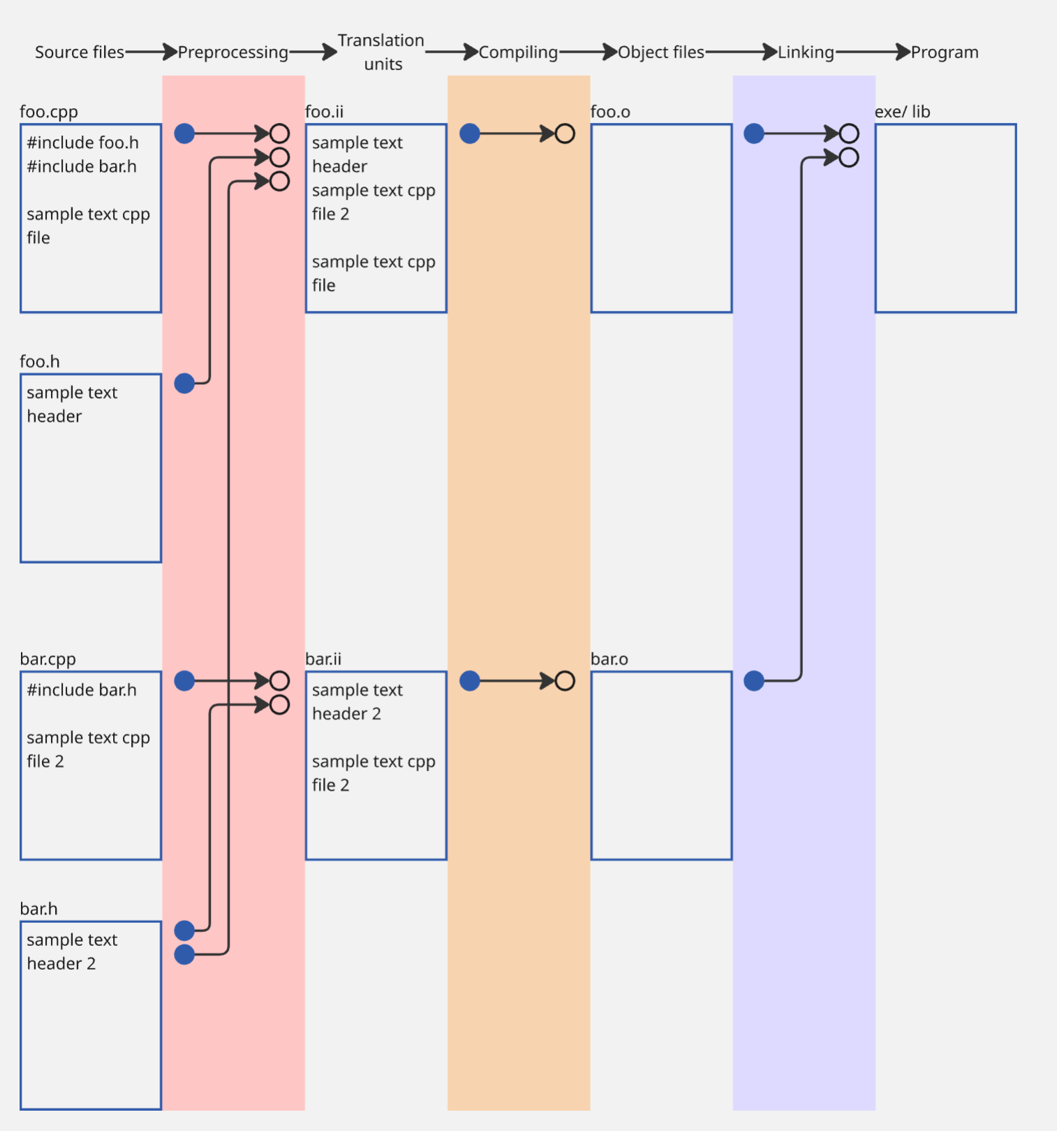
1. C++ build recap
To make sure we are starting of with the same high-level understanding of how the build process works, here a little refresher.
First, source files are passed through a text processor that copies and pasts the included file wherever the “#include” block was. For example, if I was to include #include in an otherwise empty file, the preprocessor would make it around 20.000 lines long. These are then compiled into independent object files. In the last step, the entities that are being referred from a different translation unit must be linked to create a well-formed program.
2. Storage duration
Storage duration says something about the lifetime of an object. It does, however, not say when an object will be constructed or destructed exactly, but gives a limit as to when an object may be available. There are four general categories of storage duration:
automatic
static
thread
allocated
Lifetime
local scope
program execution
thread execution
dynamically allocated
The most obvious example on storage duration I can think of is if we want to count how often a function was called:
Naturally, this does not work. Our “counter” variable has automatic storage duration and does not exist beyond the scope of the “count_calls()” function. We can change that by extending its storage duration to the whole program using the static keyword:
Associated with the storage duration are four keywords.
static
thread_local
extern
mutable
Thankfully, these follow pretty simple rules. If we have a block of code with multiple specifiers, we can simply apply the table below and stop at the first match.
staticmutableexternthread_localint j; // wrong syntax but would be thread
So far so good. But what happens if we apply the static keyword to functions, which do not have storage duration by definition. It turns out that some specifiers can not only affect storage duration but also linkage.
2. Linkage concept
As the name suggests, linkage changes something in the linking step of the build process. It describes where an entity (say a data member or function) is exposed to and can be accessed from. An entity can have no, internal, external, external weak linkage¹.
None
Internal
External
Weak external
Available to
local scope
translation unit
all translation units
all translation units
Specifiers that may affect the type of linkage are not self-explanatory:
Their effect on linkage may depend on the storage duration of the object (obviously not for functions). Specifically, static and thread storage duration lead to the same linkage rules while automatic storage duration leads to different linkage rules. Note that dynamically allocated memory using new/delete cannot be reasoned about in terms of linkage, because we only ever interact with heap memory using pointers (who’s linkage we can modify using the keywords).
¹ I am explicitly leaving out module linkage because I have not been exposed to modules enough to talk about them.
2.1 Automatic storage duration
Entities with automatic storage duration never have linkage. For example, the code below will not build because the variable counter is not exposed to anywhere outside of its local scope, it has no linkage. We can prepend static and thread_local specifiers as much as we want and change the storage duration but linkage remains unaffected.
intmain(){ // does not compile! std::cout << counter << std::endl; return0; }
2.2 Static or thread storage duration
Global variables have external linkage. This means we can access them from another translation unit. However, we need to tell compiler that the symbol is not missing but can be found in another file. For that, we must declare it in the current scope and indicate that its definition can be found elsewhere using the *extern() keyword:
Linkage interacts with the One-definition-rule (ODR), where each entity must have exactly one definition in the entire program, though it can have multiple declarations. Naturally, if an entity is not available to a scope it does not violate the ODR. For entities with external linkage, the ODR ensures that only one definition exists across all translation units, and multiple declarations (e.g., via extern) must refer to that single definition. It follows, that entities with internal linkage may be defined multiple times across the program but not within the same translation unit. The linker treats each definition unique to its file. Entities with no linkage, like those with automatic storage duration, are exempt from ODR because their scope is confined and they don’t participate in linking across units.
This is a violation of the ODR, since the global variable counter is redefined in multiple translation units and has external linkage. As expected, we get “Linker error: One or more multiply defined symbols found” and “Linker error: Symbol already defined in object” (in MSVC) for the counter variable. From our exploration of the C++ compilation earlier, we know the #include statements essentially just copy the text in the preprocessing stage. The linker does not know if a variable was copied in via an include or explicitly defined multiple times. We can resolve this by marking the variable static, giving it internal linkage:
Each file (foo.cpp, bar.cpp, main.cpp) now has its own instance of the counter variable. This can be useful if we want to share functionality but not data. Notice how the statement,
1
*thread_localstaticint counter{10};*
now makes more sense. This is a variable with thread_local storage duration and internal linkage (due to static). We will get to the precedence of multiple specifiers later. In our example, however, we probably intended to increment the same counter from different translation units. There are two ways to achieve this: First, we can have a single definition to avoid violation of the ODR together with multiple declarations with external linkage.
Here, the extern keyword tells the linker that the definition can be found in a different translation unit with external linkage. If I print the address of counter in bar.cpp and foo.cpp both are the same:
1 2
bar: 00007FF73193D000 foo: 00007FF73193D000
In C++ 17 the inline keyword was added which can simplify the code above quite a bit. The Inline specifier (in isolation) results in external weak linkage of an entity. External weak linkage works much like external linkage but allows violation of the ODR with the assumption that all provided definitions are the same. The linker will then select one definition to use (e.g., the first one it encounters) and ignore all others. This is great if we are working on a header-only library. A good way to remember this fact is by thinking of what inline also does: Hinting towards potentially inlining a the code of a function instead of creating a separate function call. If we assume the compiler always inlines everything that we mark with inline, the selected code becomes local to the scope it is used in. In that case, multiple definitions would not be a problem since the inlined variables would have automatic storage duration. In reality, how much really is inlined depends on the compiler. A quick experiment shows that MSVC barely inlines, Clang inlines a few instances and gcc is the most aggressive about inlining of the three.
Again the addresses of the counter variable match:
1 2
bar: 00007FF787BAD000 foo: 00007FF787BAD000
Variables marked a single const-keyword have internal linkage (just like static). Which only applies if the variable is not a template, not marked volatile, extern, inline or previously declared with different linkage. The code below finds different addresses (although they probably share the same initializer from .rodata which then be copied onto the stack).
Similarly, constexpr implies const and constinit for variables. Constinit says something about the compile time behavior of the program only, so the relevant part of constexpr is simply const. The only exception that I could find are static member variables and functions, for which the keyword implies inline. This makes intuitive sense, because static members, both variables and functions, are typically defined in a header file so they can be accessed from multiple translation units.
Finally, there is a trump card. We can force internal linkage of any variable or function using an unnamed namespace. Any and all specifiers we have mark our functions or variables in an unnamed namespace will have no effect. This is great to use for local objects that we don’t want to accidentally leak outside a translation unit.
Intermezzo: How to declare?
In the example introducing the extern keyword, you may have been surprised that the extern keyword was needed for the global variable but not for the free/ global functions. I.e., Why does int counter; not work?
//main.cpp voidincrement_via_bar(); // <-- but not here?
Let’s recall the declaration and definition rules.
I.1 Variables
Local variables cannot be declared without defining them. Depending on your compiler warning level, the following may not compile. Even if it does, the compiler will need to allocate memory when pushing the variable onto the stack, making this a definition. If we do not initialize, its value is indeterminate for fundamental types. The only exception that I can think of if is when the variable is unused, in which case it is probably optimized out anyways. I was able to trick the compiler using a reference decayed to a raw pointer into running this code to illustrate:
1 2 3 4 5 6 7 8 9 10 11
#include<iostream> voidfoo(int* k){ k++; } intmain(){ int k; foo(&k); std::cout << k << std::endl; //UB, I am getting -858993459 return0; }
Member variables can be declared if they are static non-const data members. Other variable types with either be zero-initialized or need explicit declaration:
1 2 3 4 5 6 7 8 9 10 11
#include<iostream> structC { staticint k; };
intmain(){ int x = C().k; // Error LNK2001 unresolved external symbol "public: static int C::k" (?k@C@@2HA std::cout << x << std::endl; / return0; }
For which the documentation says: “There are many ways to get LNK2001 errors. All of them involve a reference to a function or variable that the linker can’t resolve, or find a definition for. The compiler can identify when your code doesn’t declare a symbol, but not when it doesn’t define one.” This matches our understanding.
Global variables can only be declared without definition by using the keyword extern as we established earlier.
I.2 Functions
Global functions and Member functions can be declared as I did above.
1 2 3 4 5
voidfoo(int arg1, ...);
structC{ voidbar(int x); }
Local functions only exist in the form of lambdas and other function objects (i.e. functors) which cannot be declared. Functors behave like any other local object with regards to their lifetime.
1 2 3 4 5 6 7 8 9 10 11
#include<iostream>
intmain(){ { auto mylamb = []() {return10; }; } int x = mylamb(); // mylamb is undefined std::cout << x << std::endl; return0; }
3. Functions
So what is different for functions? Since there is no such thing as storage duration for functions, the whole problem becomes a bit simpler.
We already discussed that global and member functions have global linkage by default (just like global variables). Here, global variables needed the extern keyword to be declared (and not defined), functions do not. We also already know that constexpr implies inline for functions. We discussed that this would be useful to avoid ODR violations, since the function will likely be placed in the header file. Note that if multiple, but different definitions of the same inline function exist (e.g., one marked consteval) the program is ill-formed. In the current revision, const only has meaning on member functions, thus is redundant or may even lead to a compiler error if used on global scope. It generally has no effect on linkage of functions.
1 2 3 4 5 6 7 8 9 10
// foo.h inlineconstconstexprintfoo(int x){ // inline and const are redundant here return x; }
Just as with variables, anonymous namespaces are again are the trump card to beat all other specifiers (forcing internal linkage).
Finally, what about consteval and constinit? We already established that constinit can be thought of as the part of constexpr at compile time. This is not entirely true but a useful to relate the two keywords. Constinit has no effect on linkage. Consteval on the other hand should ideally be an “immediate function”, meaning that it has to be evaluated at compile time and consequently is not included in the object files. The standard does not differentiate between compile-, link- and runtime, so this is not guaranteed behavior. I have observed that in MSVC the function could be referred from other translation units, but would not rely on it.
4. Multiple keywords
Below I made an attempt of encoding all the rules outlined above into one big decision tree. Start from the top row and stop until you meet a keyword used. This one determines the linkage.
keyword/ linkage
No linkage
Internal linkage
External linkage
Weak external linkage
unnamed namespace or namespace access
any
extern
global function or global variable
static
global function or global variable
inline, constexpr function
any, except local variables and with ODR for inline functions
const, constexpr variables
global variables if non-volatile, non-template, non-extern
(none)
local variables
any, except local variables
Here a ridicules and example with static thread storage duration (thread_local) and internal linkage (unnamed namespace):
Unnamed namespace is the first one so we know the linkage will be internal. Without it, the linkage would be the linkage specified by extern which is also internal. Without extern, the static would force internal linkage again. Without static, inline would lead to external weak linkage. Without inline, constexpr implies const for variables which would give internal linkage again. Without any specifier, the linkage would be external.
Conclusion
Finally, I would like to stress that this blogpost and the above table specifically are tools to navigate these keywords in most cases. If we apply more strict criteria, I would argue that the C++ standard does not formally define compile-time, link-time, or runtime behaviors for linkage, nor does it recognize “weak external linkage” as a formal category. How the inline concept allows for multiple definitions exactly is a linker-specific concept (e.g., ELF weak symbols) and not guaranteed by the language, making it an oversimplification in the table.
Today, we will try to build as much of a computer as we can, starting with some elementary building blocks.
When I assembled the parts of a computer for the first time, it felt like I was an expert on computers. I was telling all my school friends about CPUs and GPUs and RAM without knowing much beyond single sentences such as “The CPU is like the brain of the computer.”, or “RAM stands for random access memory”. Random access, that seemed useless why would anyone want that? So today, we will shed some more light on the magic box that I am typing this on.
Where to start?
As a child I liked to ask “why” in response to any answer I got to my initial question. As an adult, I feel not much different. However, I am more aware of the complexity of things and will need to get over myself and make some assumptions. Otherwise, we would be starting at physics topics I am not really interested in with regards to the current question. Also, this read would become infinitely long.
So let’s start with some assumptions:
Electricity works like water in my head. If I turn the tap on, the water runs. If I turn it off, it does not run. For our task, this should be good enough, but please know that there is more to it.
We also assume a few fundamental things already exist. Most notably, we will skip over the circuit logic needed to implement the NOT- and AND-Gates.
Occasionally, I felt that I needed to brush over and ommit details to aid the consistency and length of this post. If you are not satisfied after reading - great! How about you start with one of the sources I linked at the end? If you find something is that is incorrect (which is very possible), send me a message on Linkedin!
Goal 1: Invert inputs.
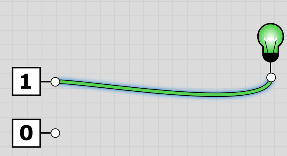
Let’s start with a simple idea: I get electricity out of my socket. Let’s visualize this:
I decided that when the electricity tap is open, I will mark this with a 1. If there is no electricity running, we mark it by 0. This is important.
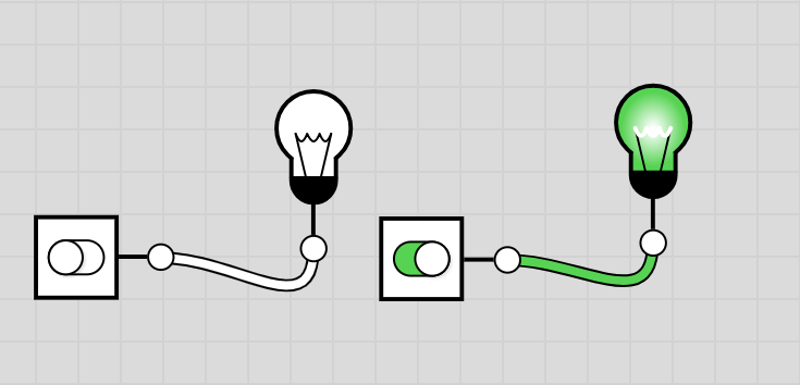
Now, I assume that we can have a switch that can turn this electricity off and on.
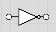
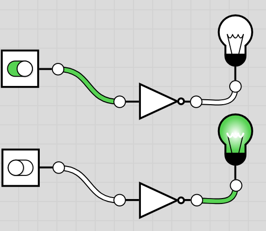
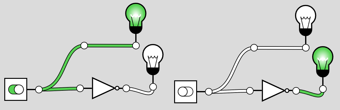
Not much so far. Let’s introduce a few new things. First up, the NOT-gate.
We can use this to invert the signal. If the water is flowing, this stops it. If the water is not flowing, this starts flowing. In the case of water, this is essentially magic. We could imagine this as a flood gate with two incoming streams. One visible that we see in the picture and a second one that is always flowing. If our first stream (the one control with the switch) is running, the floodgates stay shut. If that stream dries up, however, we let water run from the infinite second flow. In this triangle symbol, notice the small dot at the end of the triangle. This one will be important later.
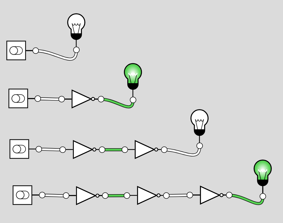
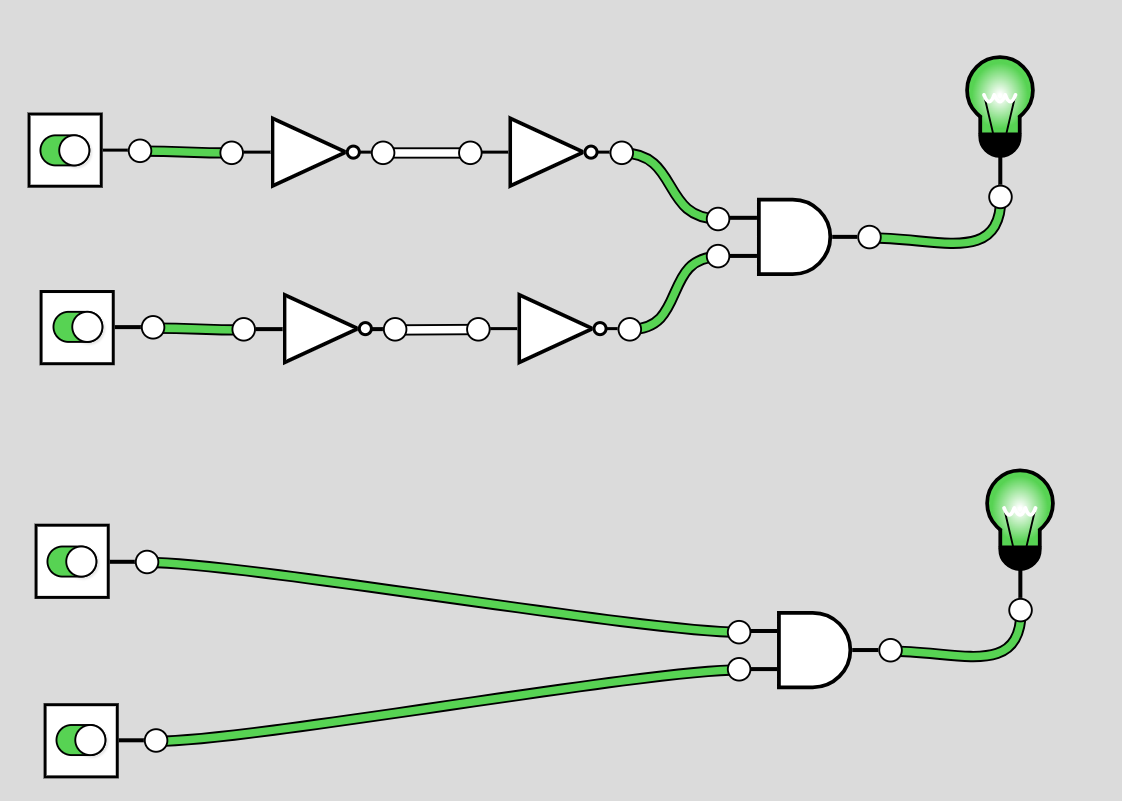
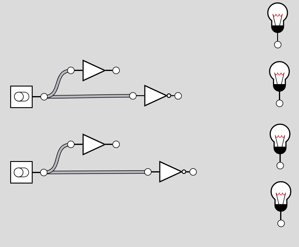
I think most won’t need convincing that inversion of inversion does nothing. That is, chaining two NOT-gates together is the same as not having any NOT-gates. In fact, we can generalize this and say that input is only inverted if there is an uneven number of NOT-gates in the system.
Goal 2: Combine Inputs
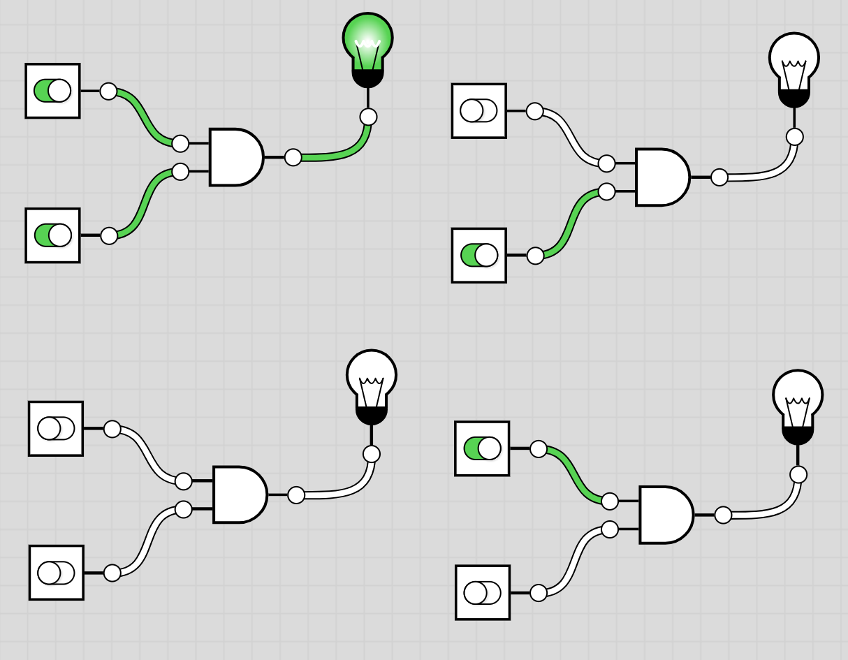
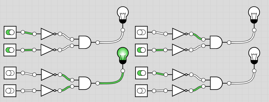
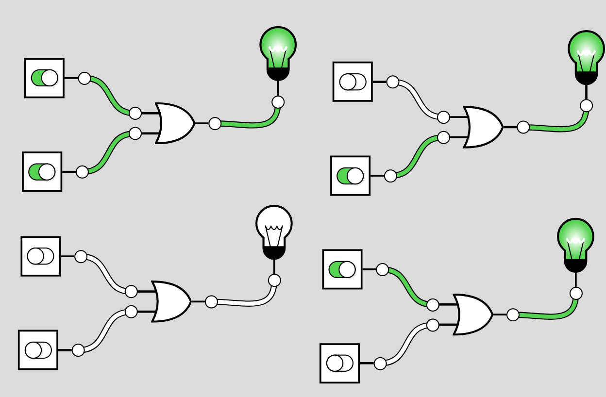
Let’s also introduce a second magic item. The AND-gate. This gate takes in two inputs like many other gates we will see. It then answers the question: “Are both inputs on?”, returning the answer as an output. If both are on, the AND-gate gives us 1 as output. Water is flowing. If both inputs are off or only a single one is on, the AND-gate returns 0.
We will use this funny-looking symbol for it. Flat on the input side, round on the output side.
We can write this “logic” down in a so-called truth table:
Input 1
1
0
0
1
Input 2
0
1
0
1
Output
0
0
0
1
Similarly, for the Not-gate:
Input 1
0
1
Output
1
0
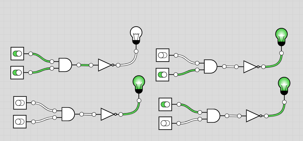
Goal 3: The NAND-Gate
Now that we can combine and invert inputs, let’s play around with it a bit. If we just take a single AND for now, we can combine it with a NOT gate on its output. Can you guess what happens? Which outputs in the above truth will be on (1), which will be off (0)?
In this case, the obvious answer happens to be the correct one: the output is simply inverted. All 0s are replaced with 1s and vice versa.
With the associated truth table:
Input 1
1
0
0
1
Input 2
0
1
0
1
Output
1
1
1
0
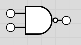
We will make this a new component called the NAND- (not-AND) gate. Now, to give it a fun symbol, let’s combine the dot from the NOT-gate and put it on the output side of the AND-gate:
The circle now indicates that the symbol is the same as the one it was based on (AND-gate), but the output is inverted.
Goal 4: The NOR-gate
Okay, by inverting the output of the AND gates, we can build NAND-gates. But what about inverting the input on the AND gate? That is, what happens if we invert both inputs? (We will invert a single input later, be patient.)
With the truth table:
Input 1
1
0
0
1
Input 2
0
1
0
1
Output
0
0
1
0
Okay, this reminds me of the AND-gate’s truth table. It seems like the output is only on when both inputs are off. Using only the AND-gate, the output was only on when both inputs were on. Somehow, this is also inverted, but differently.
The symbol of this gate looks like this:
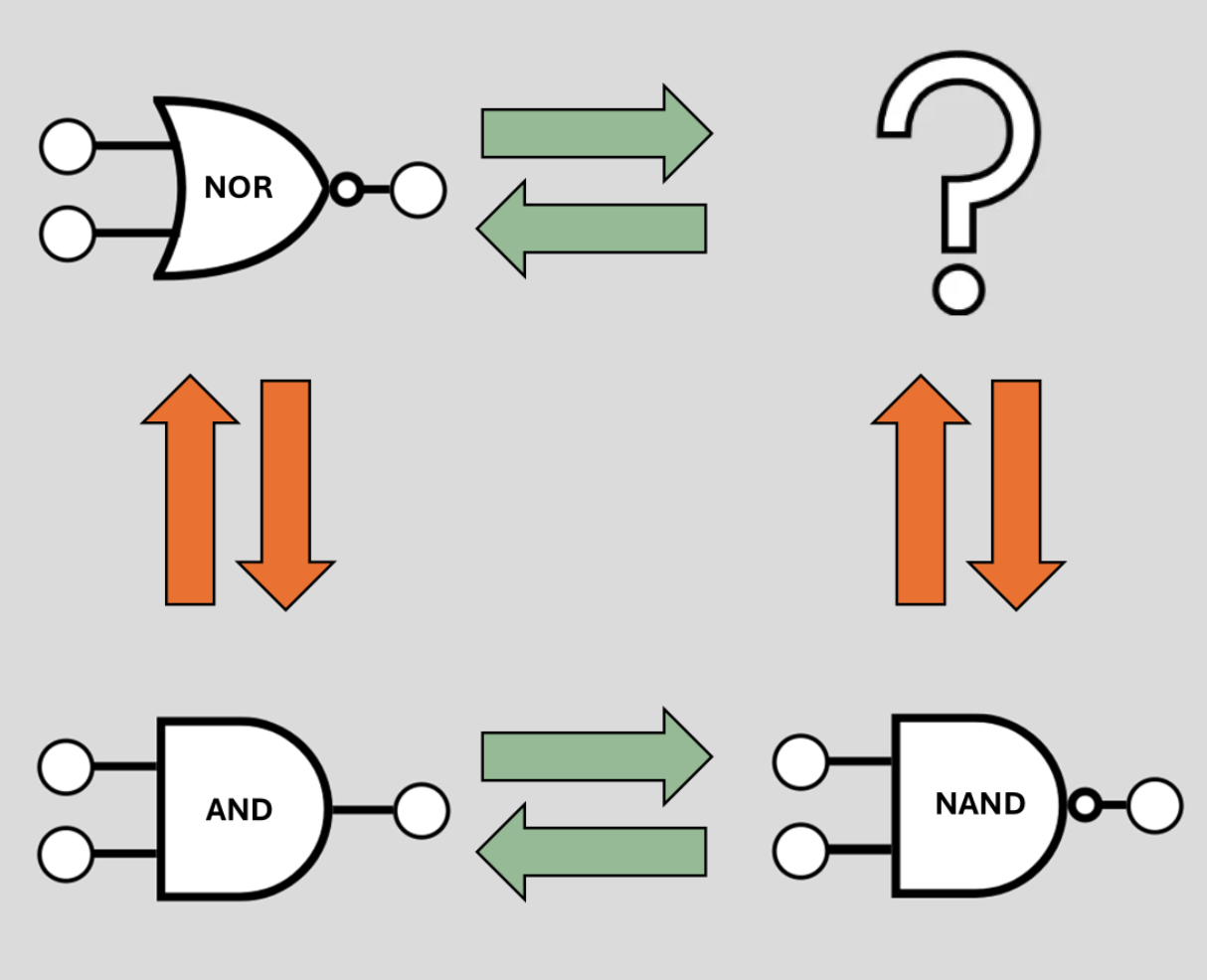
Which really does not make any sense without us first looking at how the gates we discovered relate. Let’s draw the relationship we observe out.
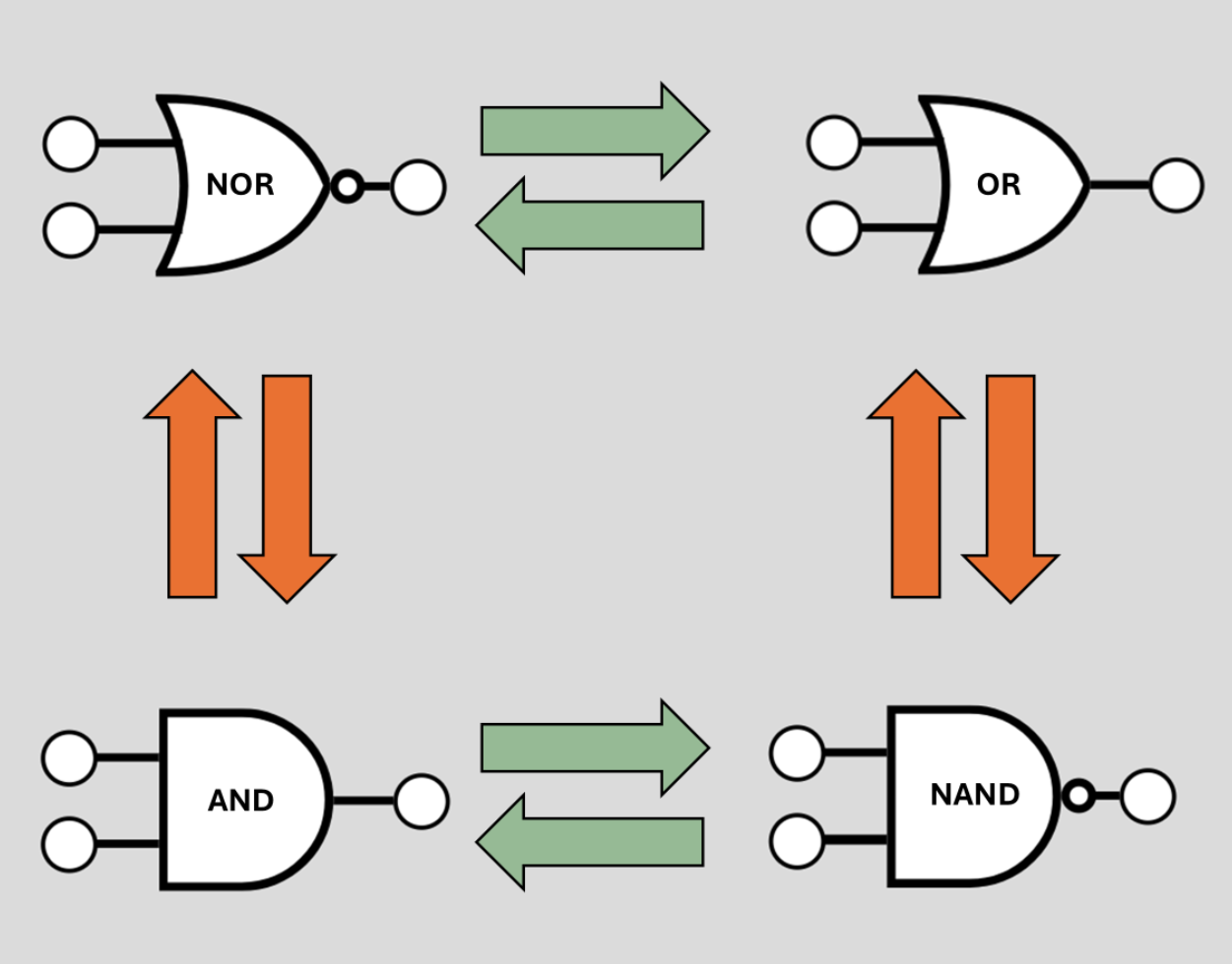
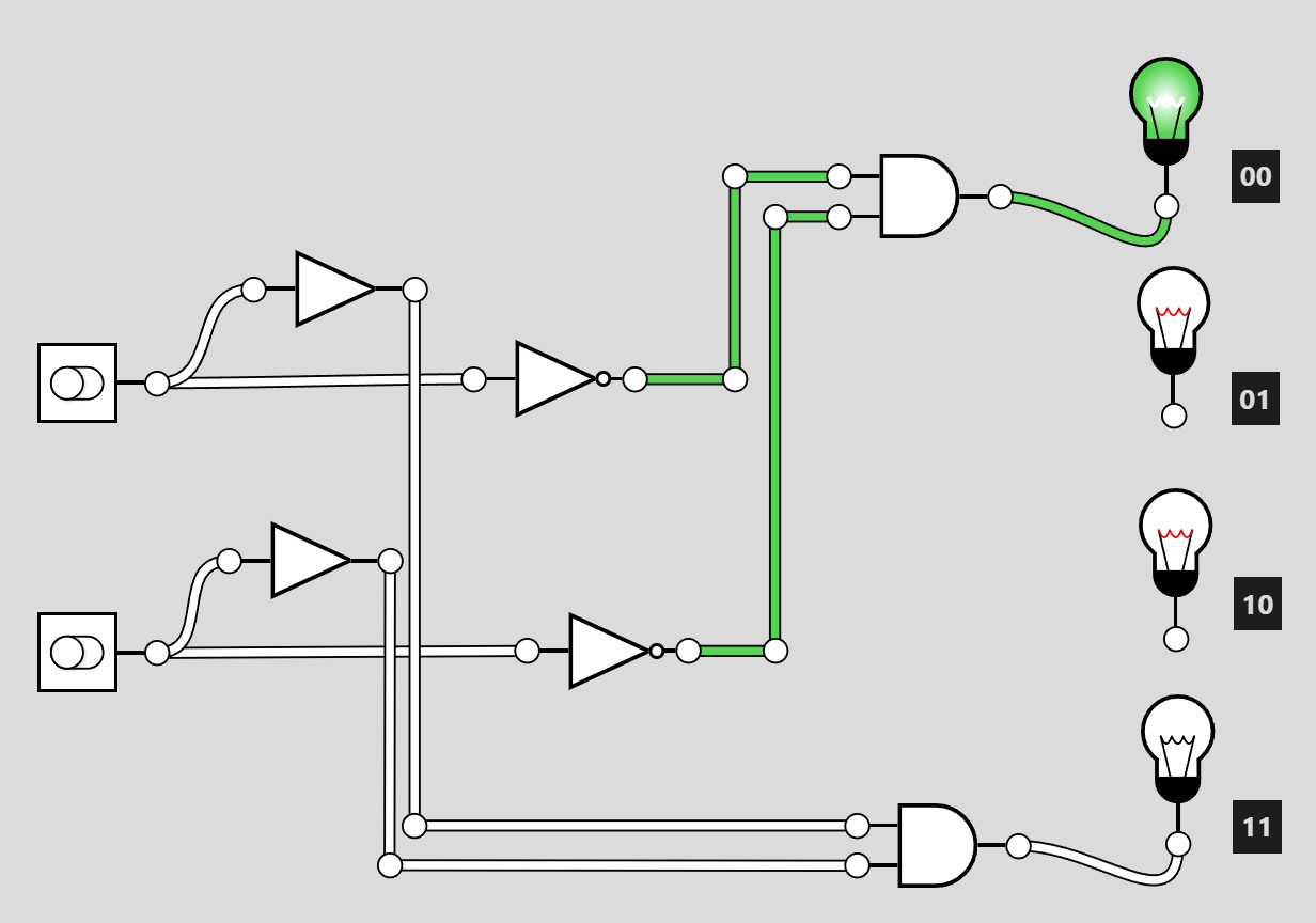
Goal 5: De Morgan’s Law (1/2)
Starting from the bottom left, we have our AND-gate. If we invert the output, we get the NAND-gate. So far, so good. Green arrows indicate inversion of output. Orange arrows inversion of input. If we invert both inputs on one gate, we travel back and forth along the orange arrows. One NOT-gate at the time. If you remember, the chaining even numbers of NOT-gates has the same effect as no not gates. This also makes sense in the picture below, where I get back to the same gate if I apply the same inversion again.
This is very cool I think, but it seems like there is a gate missing: What happens if I invert the output of the NOR-gate or equivalently invert the input of the NAND-gate?
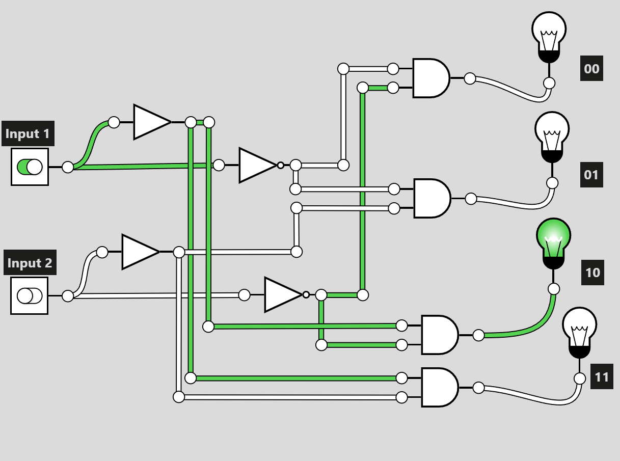
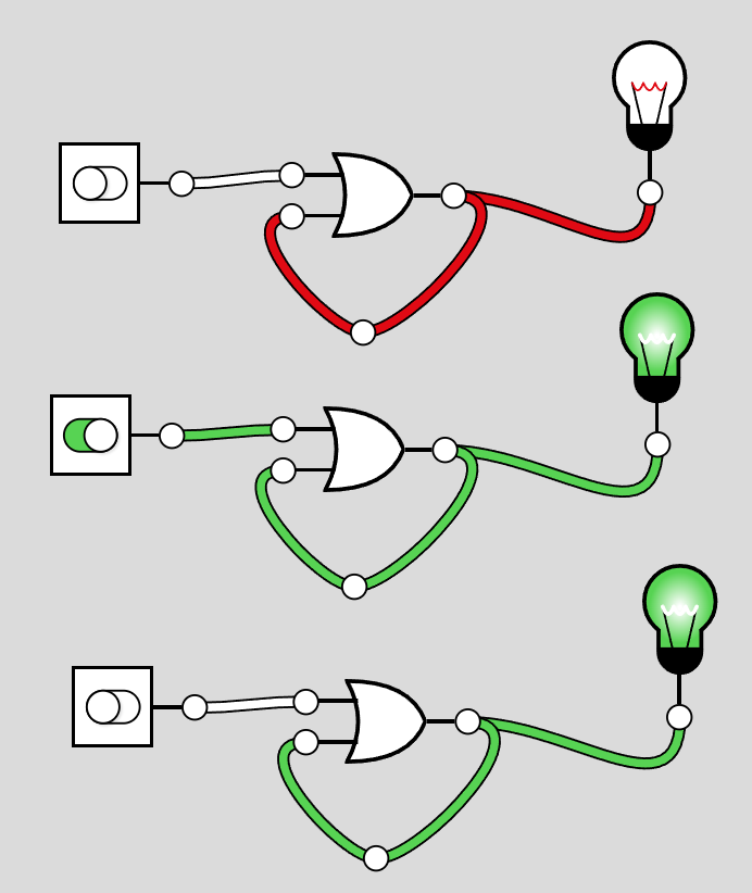
Goal 5: OR-gate & De Morgan’s Law (2/2)
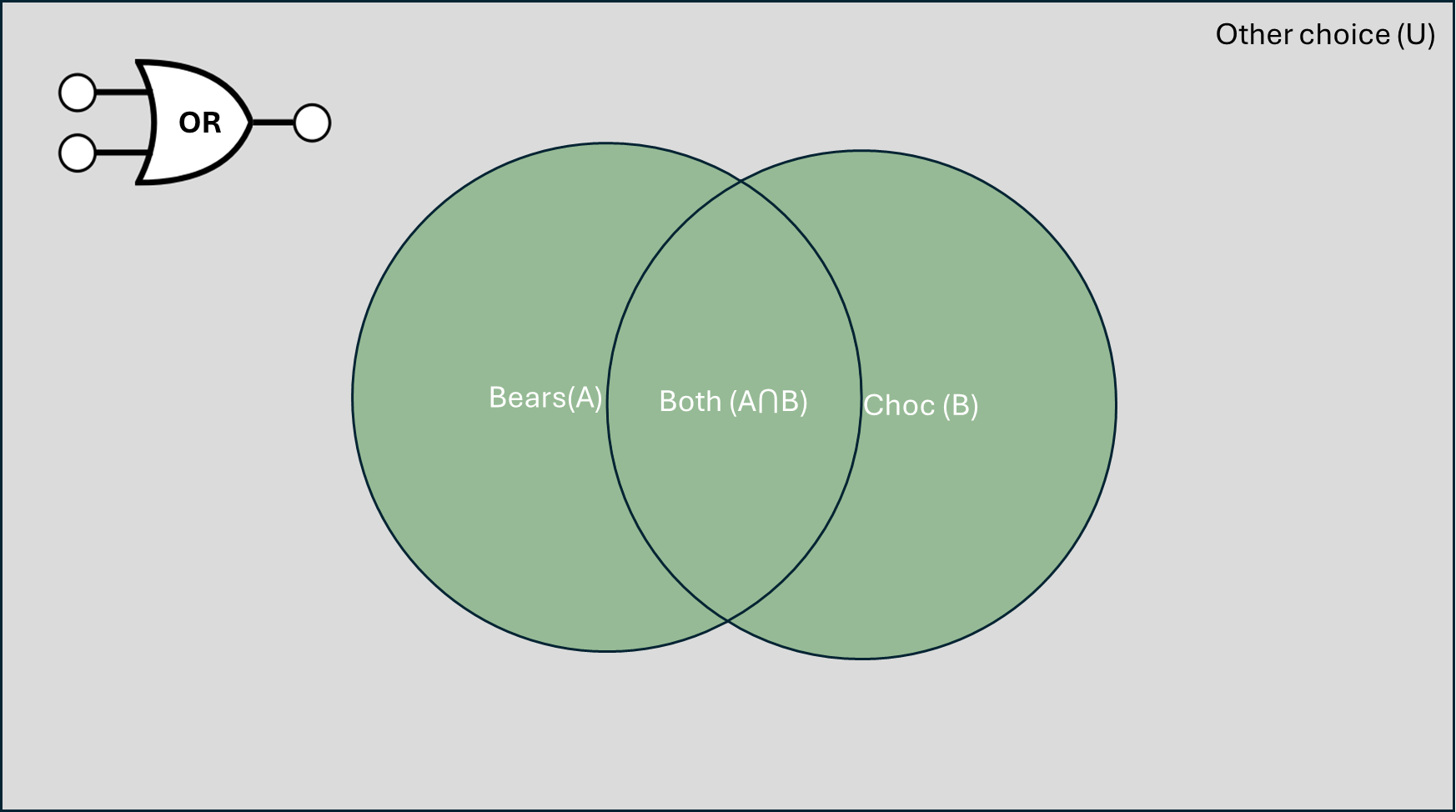
The answer is we get the “at-least” GATE, or put more simply the OR-gate:
This is the Gate that I used as a child when my mum told me that I was allowed either chocolate or gummy bears at the supermarket, but I chose both. Clearly, she was unfamiliar with Boolean algebra. Note: Can you draw out the truth table she wanted instead?
Back from my digression, we are able to complete De Morgan’s law now by placing the OR-gate in its slot.
The OR-gate’s associated truth table is:
Input 1
1
0
0
1
Input 2
0
1
0
1
Output
1
1
0
1
The dot at the end of the NOR gate also makes more sense now. It’s simply the OR-gate but with its output inverted. From what we saw thus far, the order of NOT- and AND-gates matters. Inverting the input to a gate must not be the same as inverting its output.
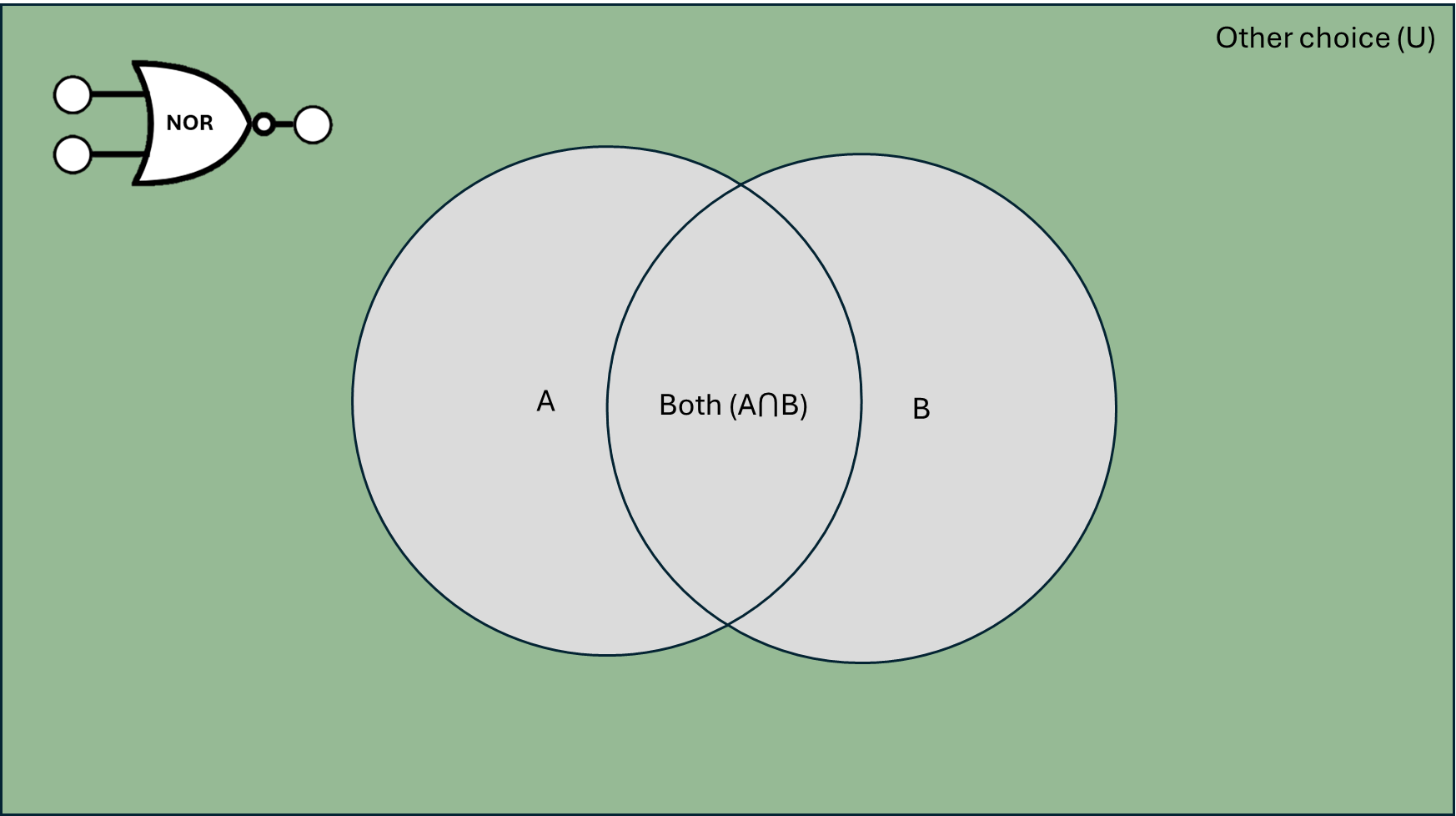
Intermezzo: De Morgan’s Law in set theory
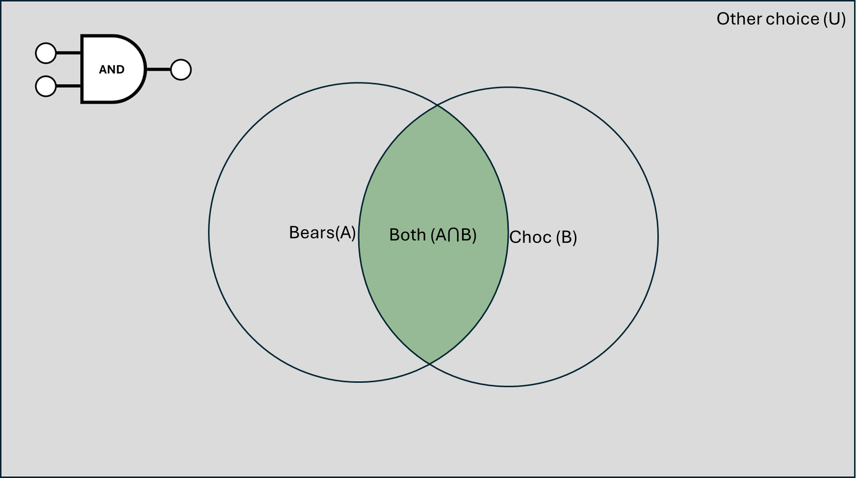
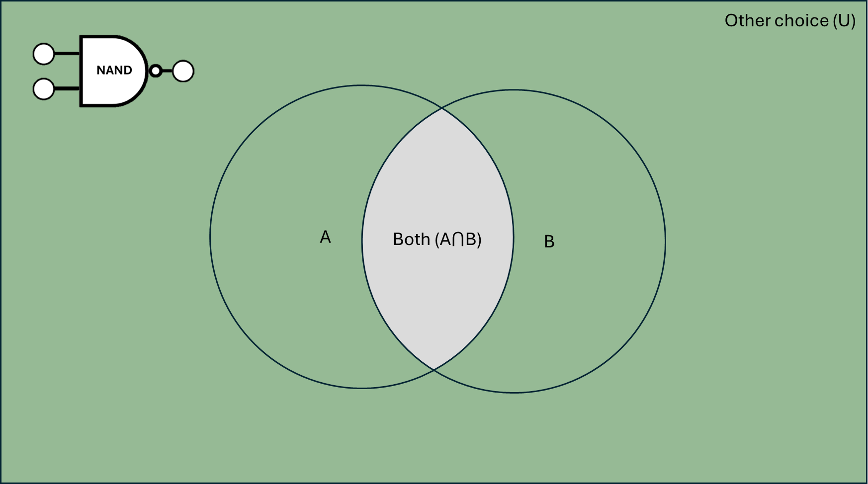
All the gates above are already highly exciting I know, but believe it or not we can do even more fun things with them. Each of them can be represented as a selection from some collection of unique elements (i.e., a set).
If I have the set of S = {choosing gummy bears, choosing chocolate}, then we can display the space of all possible choices in the supermarket in a Venn diagram: Choosing gummy bears (A), choosing chocolate (B), choosing both (C) or choosing none of those options (U). In the below graphics, green = selected (1), purple = not chosen (0).
It becomes a bit clearer what my mum meant: choose A or B but not the intersection A ∩ B. Good to know, maybe a bit late for me but better than never.
Goal 6: Making mum happy, the XOR gate.
I’ll try to redeem myself by implementing a gate that satisfies what Mum meant. Let’s start the other way around this time. Here is the truth table we want to have:
Target Truth table:
Input 1
1
0
0
1
Input 2
0
1
0
1
Output
1
1
0
0
We can chain different gates behind each other to exclude and include different parts of the set. My first thought is to start with an OR-gate. Its truth table is very close to what we want, except for the both-1-situation.
OR-Gate Truth Table:
Input 1
1
0
0
1
Input 2
0
1
0
1
Output
1
1
0
1
Now we could combine this with a gate that has the opposite behavior. We need to somehow isolate the case where both inputs are 1. The gate we need is the NAND gate.
NAND-Gate Truth table:
Input 1
1
0
0
1
Input 2
0
1
0
1
Output
1
1
1
0
We want both conditions to be satisfied. Both the condition of the OR-gate and the NAND-gate. As the sentence suggests, we can use the AND-gate to test if both conditions are met:
Great, this is what she was referring to: the exclusive OR-gate: the XOR-gate.
XOR-Gate Truth table:
Input 1
1
0
0
1
Input 2
0
1
0
1
Output
1
1
0
0
What we built makes intuitive sense to me, but it may not be the shortest representation of this logic. If we need to build everything out of NAND and NOT gates, we need 3 NAND gates and 5 not gates:
NAND gates needed
NOT gates needed
AND-gate
1
3
OR-gate
1
2
NAND-gate
1
0
TOTAL
3
5
We can do better by just using 4 NAND or 5 NOR gates.
We can represent the same logic in different ways. I am sure the people designing CPU’s are thinking about this a lot. Let’s leave it to them for now.
Goal 7: Are on/off states actually numbers?
So far we have been working with off and on states only. If we rethink that in terms of numbers, we get only two possible numbers 0 and 1. Let’s see what numbers in base ten (decimal) we are able to represent in this binary (meaning “two together”, “a pair”) system:
Decimal (0-9)
Binary (0,1)
0
0
1
1
2
?
We can name this single digit binary number a “bit”. I happen to use numbers larger than 1 on a daily basis, so how can we represent them here?
In decimal, we actually have the same problem: We use higher numbers than 9 by just resetting the spot the 9 was in to 0 and incrementing the spot before it: 09, 10, 11, 12, etc. Let’s use the same approach in our binary system:
Decimal (0-9)
Binary (0,1)
0
0
1
1
2
10
3
11
4
100
5
101
6
110
7
111
8
1001
9
1010
10
1011
…
…
With every extra digit in the decimal system, we can represent 10 times more numbers: with 1 digit we can represent 10 numbers (e.g., 0-9), with 2 digits 100 numbers (e.g., 0-99), with 3 digits 1000 numbers (e.g., 0-999) etc. The formula for how many digits we can represent with digits is . In binary, this works the same, but now we replace the ten with a two: . We can cross-check our understanding with the table above. With a single digit, we can represent two numbers: 0, 1. With two digits, we can represent numbers: 0,1,2,3 in decimal. Notice how the largest number is one lower than the total numbers that we can represent: With 2 digits, hence 4 numbers we cannot represent 4 if we want to represent 0, 1, 2, and 3. Similarly in decimal, with ten numbers we cannot represent a ten with a single digit. The formula for the largest number that we can represent with digits is therefore .
Now that on and off states are suddenly numbers and not mere categorical states anymore, we can try to think about what we can do with those numbers.
Goal 7: Half adder
Thinking of the on/off states as numbers gives us some ideas of what we expect to be able to do with those numbers. For example, how could I add two numbers together in this system?
Let’s use an example:
Decimal (0-9)
Binary (0,1)
0 + 0 = 0
0 + 0 = 0
0 + 1 = 1
0 + 1 = 1
1 + 0 = 1
1 + 0 = 1
1 + 1 = 2
1 + 1 = 10
Alright, so the largest number we can have in binary is unsurprisingly 1. The smallest number that we can add that actually changes the number happens to be 1 too. This seems a bit annoying, but actually makes things very easy. Let’s try to build a small calculator for a single digit. We know the largest number that we can get with two digits in binary is 2, that is 10 in binary. So we know we need two output slots, one for the left-hand number and one for the initial digit on the right-hand side.
Let’s think about how to calculate the right spot first using a familiar tool: the truth table.
Input 1
1
0
0
1
Input 2
0
1
0
1
Right-hand number output (SUM)
1 (1+0)
1 (0+1)
0 (0+0)
0 (1+1= 10)
Left-hand number output (CARRY)
0
0
0
1
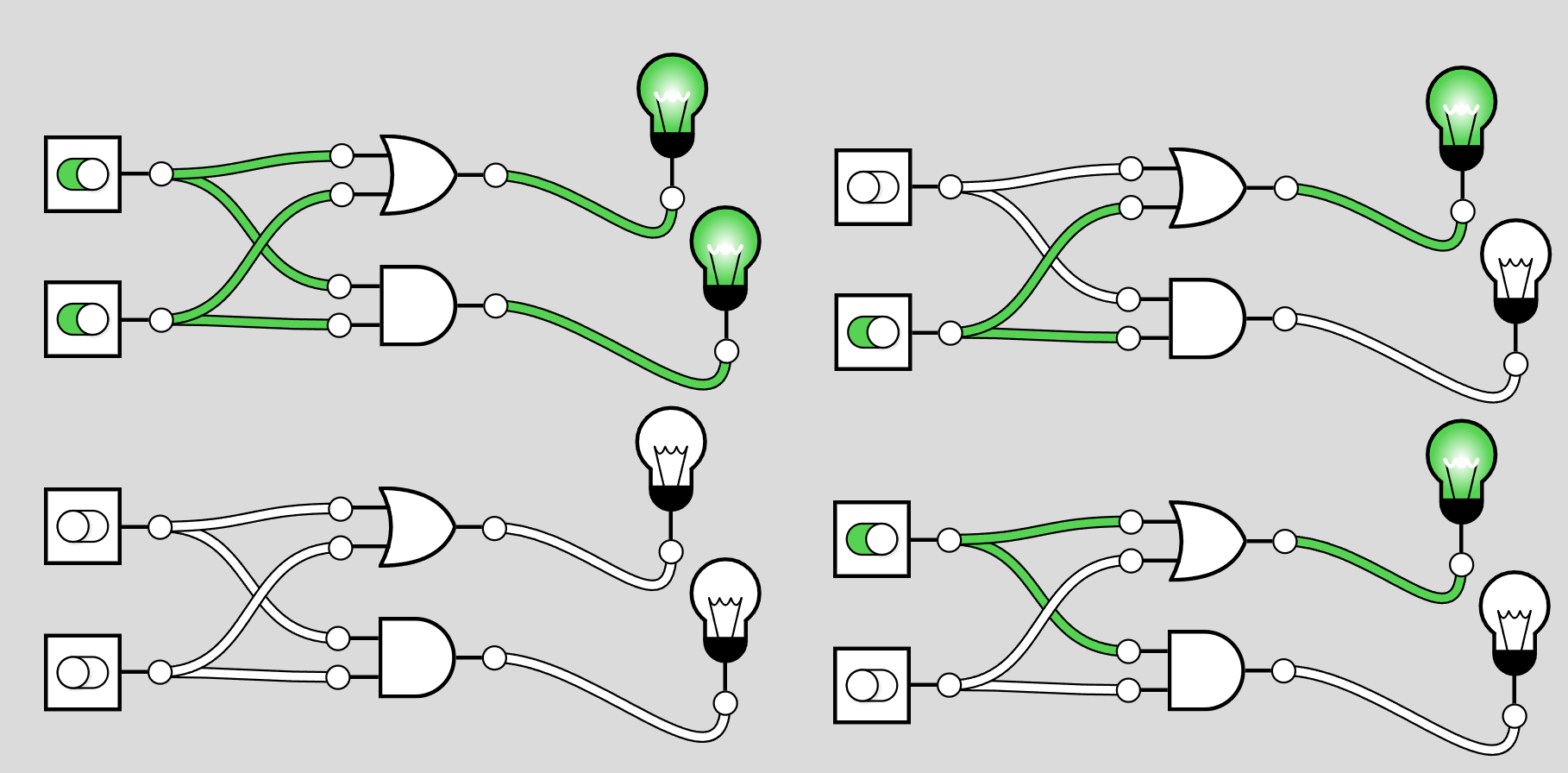
Do you see a familiar pattern? Which logic gate almost magically matches this truth table? The answer is that addition in binary for the right-hand number is the same as the OR-gate. Similarly, the output pattern we need for the left-hand digit matches the AND-gate. We can rename those to match the naming standard we are used to from primary school studies: Sum and Carry.
Let’s draw up this circuit and have a look at all possible states:
The upper light bulb represents the SUM output, the lower lightbulb the carry output. Seems to work well for a single digit. I think we are ready for the next step. How about we try to impress our coworkers and add digits larger than one and zero?
Goal 8: Full adder
We would like to chain the above circuits together in such a way that we can compute the value of each digit in our number from the previous digits. Much like in addition to paper, we need to consider both numbers and also the carry from the digit at the position below.
We could try to write down the truth table for this, but then we would need three inputs and two outputs. This would lead to 9 columns, which I cannot be bothered to draw out. Instead, let’s see how far our reasoning can get us.
First, if all values are zero, nothing happens. Secondly, if any of the three input values are 1 but the others are 0 there won’t be any carry. So far, so boring. Thirdly, if two of the three input values is 1, then we will definitely get a carry value because we know that 1+1 does not fit into a single digit (i.e. bit). In this case, those two will make the SUM value 0 + x, where x is the value of the last input.
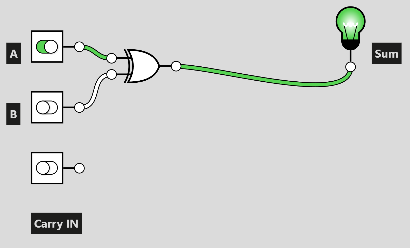
To simplify the problem, we can just work on one part first: the SUM.
Calculating the SUM
We can start a bit silly and just chain two OR-gates. After all, this worked fine for two inputs and I said that the OR-gate is equivalent to Addition.
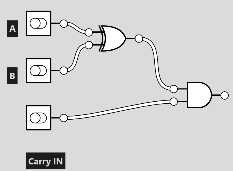
Thankfully, it’s not so simple and a bit more fun is involved. The OR-gate also outputs 1 if both the inputs are on. But now, we only want it if one of them is on. Let’s think back to what we want: Either one or three of the inputs are 1. Let’s simplify the problem even further, let’s assume we know the carry is 0. Then we know the truth table we need:
Input 1
1
0
0
1
Input 2
0
1
0
1
Output
1
1
0
0
Which we recognize as the XOR gate:
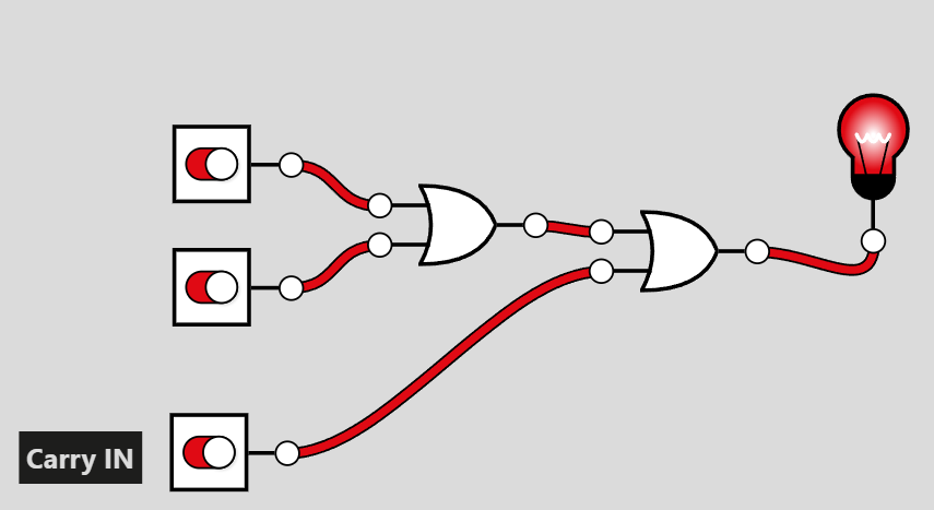
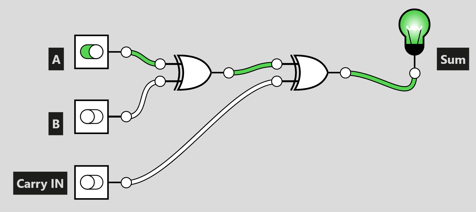
Great, now we also need to test if either this case happens or (exclusively) the carry is 1. We can do this by chaining a second XOR gate behind the previous one.
Computing the CARRY
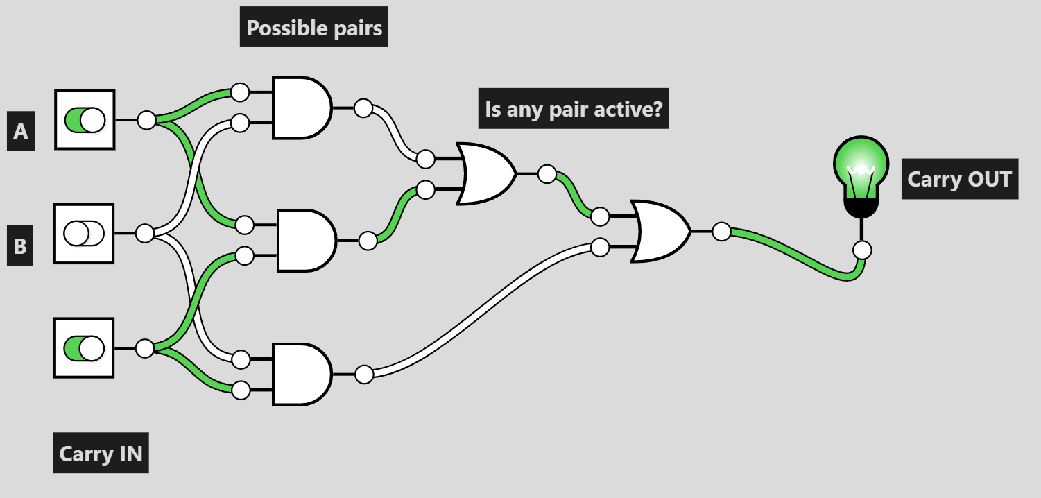
I am thinking about in which cases there will be a carry. If all values are 0 then, there obviously won’t be any carry. A carry can only appear when at least two of the bits we are adding are 1. This makes sense, because 1 is the largest number we can represent with one bit (in our coding scheme). So, for the carry, we will essentially have to answer the question: “Are there at least 2 inputs equal to 1?”. Or phrased differently: “Is there any pair of inputs on?”.
Finding pairs is not so difficult, we already did this in the very first task using the AND-gate. Let us then make an AND-gate for all possible pairs and then check if any of those are on. This “Any” relationship we are looking for, we can represent with OR-gates. We don’t mind if there are multiple pairs that are turned on, because this only indicates that 3 of the inputs are on and we want a carry in that scenario too.
This looks fun and simple enough, but let us think about it a bit more. Could we maybe reuse some of the logic we used in the SUM part of the adder? We know that the XOR-gate is only active when there is exactly one of its inputs equal to 1. We can limit the problem space again by assuming one of the inputs is off. Then we could use the first XOR-gate to answer the question “Is there only one of the inputs equal to 1?”. We can then check if the carry AND the XOR-output is off to check two pairs at once!
If all three of the inputs are on, the XOR-gate will output 0 and the AND gate above will not activate. We can fix this problem and test the last pair in one go, which we can do as I did in my initial idea. Then we test if either of those two pairs is active using an OR-gate as before. The OR-gate does not care how many inputs are active, so we can happily feed it two active pairs.
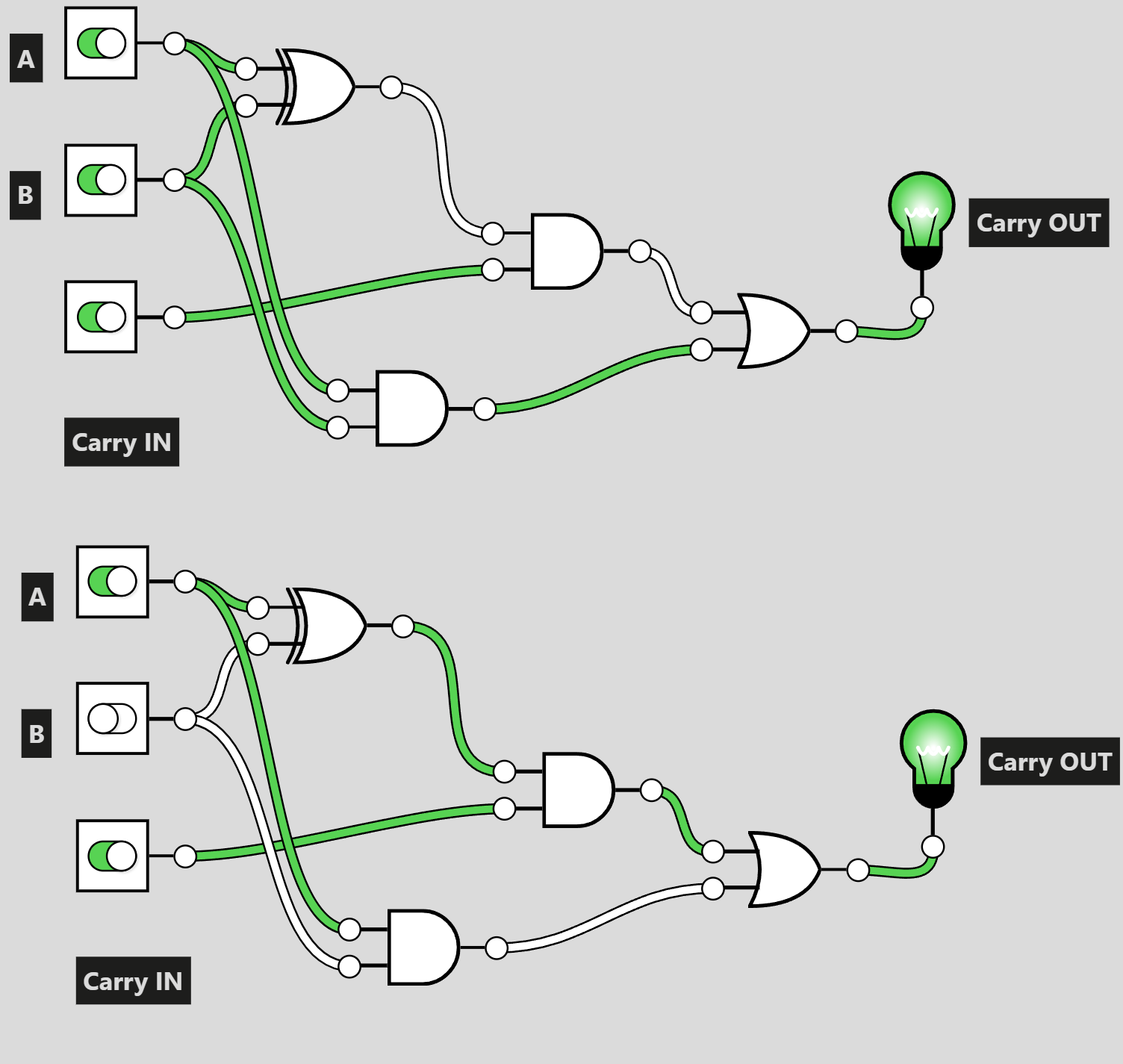
Great, we can now add 3 bits together, which is perfect to compute the carry from the bit on the position right before this one. Let’s try to stack these so that we can add numbers with multiple digits together.
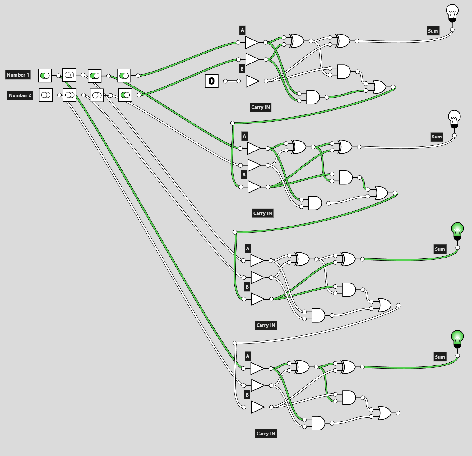
Goal 9: 4-bit adder
This may look a bit messy, but is just the same as we did before. We can now add two numbers, by adding them together position by position. For example, here 1011 and 0001, which in decimal are . The fun thing here is that we get two carries, one at the second position and another one at the third position. The second observation here is that the first adder is getting a constant 0 input for the carry. This makes sense since there was no previous position. We could actually just replace it with a half adder, but I wanted to keep it consistent. Lastly, the last carry is going into nowhere. We will always have this problem if we restrict the number of digits. We know that for 4 bits like below, there are numbers we can represent, with 15 being the largest. If we get a result larger than this, the calculation is not correct. We get integer overflow.
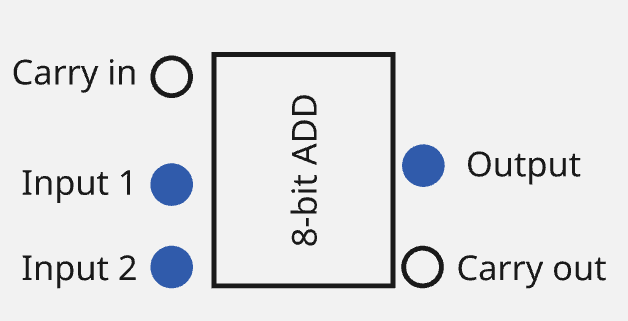
The 8-bit version of this module will be useful later:
Note that this “Ripple-Carry Adder” (https://www.sciencedirect.com/topics/computer-science/ripple-carry-adder), clearly is not the most efficient. Computing the most significant bit (bit at largest position) needs all previous operations to be completed. The longer the integer we feed into the system, the longer the idle time of components (i.e., processing time grows linearly, ).
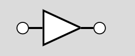
Also notice how I added the non-inverting version of the NOT-gate: The non-inverting buffer,
which, for our purposes, will not do anything. It takes the input and simply forwards it.
Goal 10: Negative numbers
10.1 Sign-magnitude representation
There are various ways of expressing negative numbers in binary. The simplest way I can think of is flipping a single bit (let’s take the most significant one) to indicate if a number is negative (1) or not (0 and positive numbers). For example, with a 4-bit integer, we could only use the 3 least significant bits to actually store any information.
This is called sign-magnitude representation. Can you guess what the problem is now? Which numbers can we represent?
This representation alone is a bit annoying to deal with because now we have two zeros:
Let’s now try to do addition:
That’s not very convenient at all if I want to do calculations. I am sure there is a way to resolve this issue, but maybe there is a better approach to this. Now, what do I have to do to make addition intuitive? That is, how can I represent it as a series of bitwise operations that are simple and fast?
10.2 One’s complement
Let’s think about how we are used to this in the decimal system. Subtraction is the same as addition but with the second number inverted (by multiplication by -1). For example:
Let’s try to define the inversion operation with the bitwise NOT-gate like we are used to. All 1s become 0 and all 0s become 1:
Adding both numbers together using the Adder we made before gives us:
The leading 1 in the result is our carry, which we toss away in our 4-bit adder. The result having a non-zero carry on the most significant bit is called overflow. Using this logic, we notice that:
Decimal
Binary
Inverted Binary
0
0000
1111
1
0001
1110
2
0010
1101
3
0011
1100
4
0100
1011
5
0101
1010
6
0110
1001
7
0111
1000
Now addition is simple between some numbers but does not really work out how we would want between all. For example:
, which after dropping the leading carry, would just be zero. This obviously makes no sense. We could try fixing the situation by wrapping the last carry around the end to the least significant bit, resulting in . Still, we would be left with two zeros, a positive zero and a negative zero. This is confusing, to say the least.
Two’s complement
We can combine both previous ideas into one. We start with One’s complement, but now instead of wrapping the carry of the largest number around, we just always add 1 after the inversion.
Decimal
Binary
Inverted Binary
Inverted + 1
0
0000
1111
0000
1
0001
1110
11111 (-1)
2
0010
1101
1110 (-2)
3
0011
1100
1101 (-3)
4
0100
1011
1100 (-4)
5
0101
1010
1011 (-5)
6
0110
1001
1010 (-6)
7
0111
1000
1001 (-7)
8
1000 (-8)
In this system, we notice two things. First, to get more negative numbers, we need to count down from 1111. This leads to the largest negative number being 1000. Secondly, at the cost of having only one zero, we now have one more negative number than positive numbers (i.e., the 8). This system of describing negative numbers is called two’s complement. The circuit that implements this inverts all bits of the input individually using NOT-gates and then uses the adder circuit from before to add +1. This “negator” circuit for 8 bytes will be represented as such:
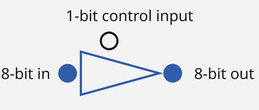
Goal 11: Tri-state buffer
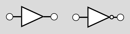
We will need a new basic magic component for our later implementations. The tri-state buffer. This component sounds more fancy than what it is: A flood gate with a control input.
We already got to know the non-inverting and inverting (NOT-gate) buffers:
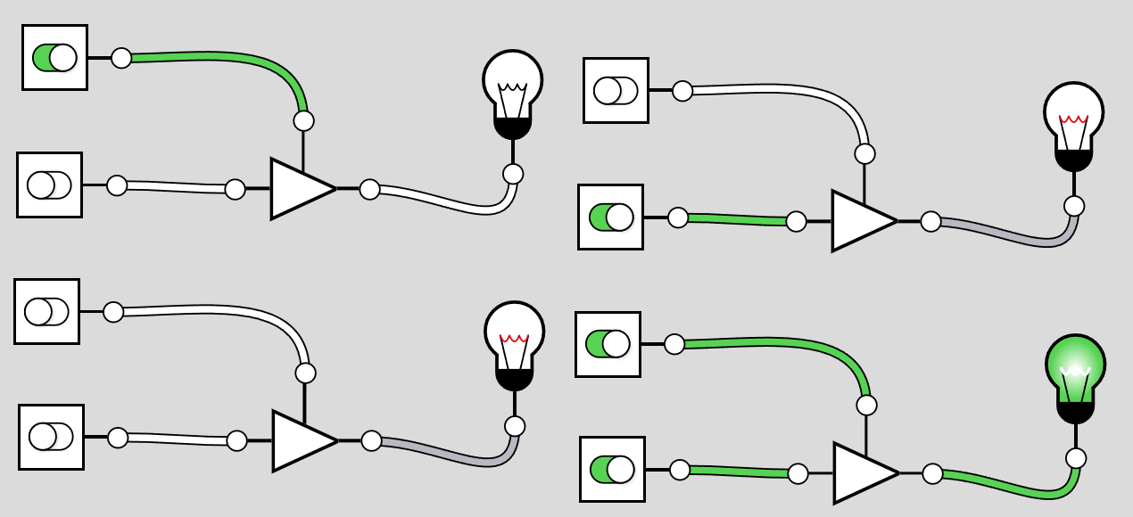
The tri-state buffer works similar to the non-inverting buffer but has a second, control input. If the control input is not on, the gate is disconnected and does not send any 1 or 0 signal down the path. Instead, it sends a third (hence tri-state) type of state, the Hi-Z state. This opens the output channel up for other gates to input without short-circuiting the system. We can imagine this as the wire being cut through. Here, the associated truth table:
—
Data Input
1
0
0
1
Control Input
0
0
1
1
Output
Hi-Z
Hi-Z
0
1
We can obviously chain these tri-state buffers to use a single control bit signal to turn a series of inputs on and off. From now on, I will try to wrap components into more abstract representations that we can use in our computer later. Here the 8-bit tri-state buffer:
I will be highlighting bytewise (e.g., 8-bits at once) with blue fields.
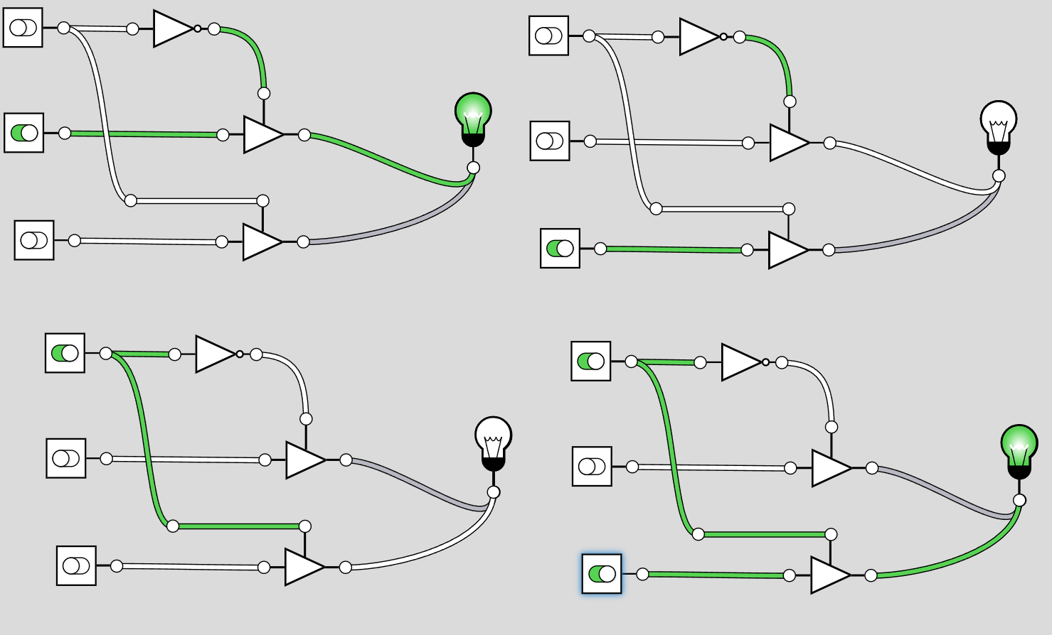
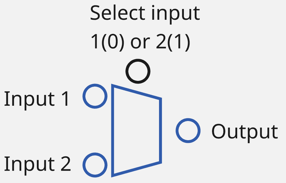
Goal 12: Data selector (MUX)
We can use this newfound item to build an input selector. That is, a new component called a Multiplexer (i.e. MUX) that will be able to select between two inputs based on a third. We can use our new tri-state buffer for this.
We want one of the tri-state buffers to return Hi-Z while the other one is passing through the input as follows:
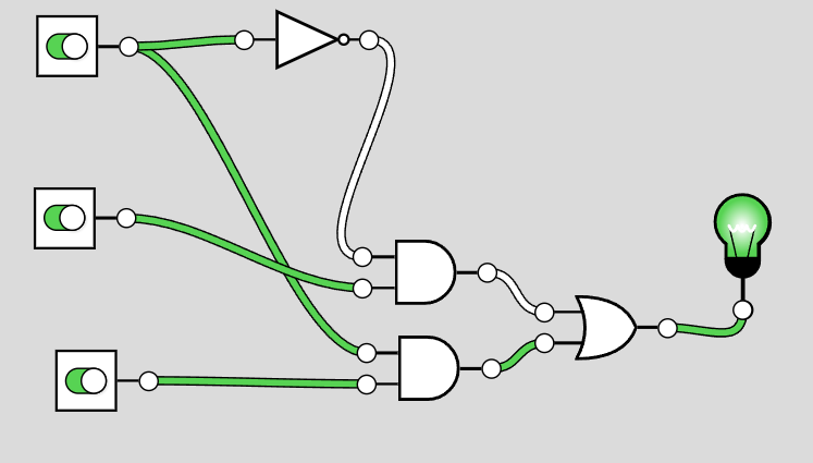
Alternatively, we could also have used gates, which does use a bit more space:
Note that we are able to chain these two-input multiplexers behind each other to act as a multi-input selector. For now, let’s create a abstract representation of this block for 8-bit data again:
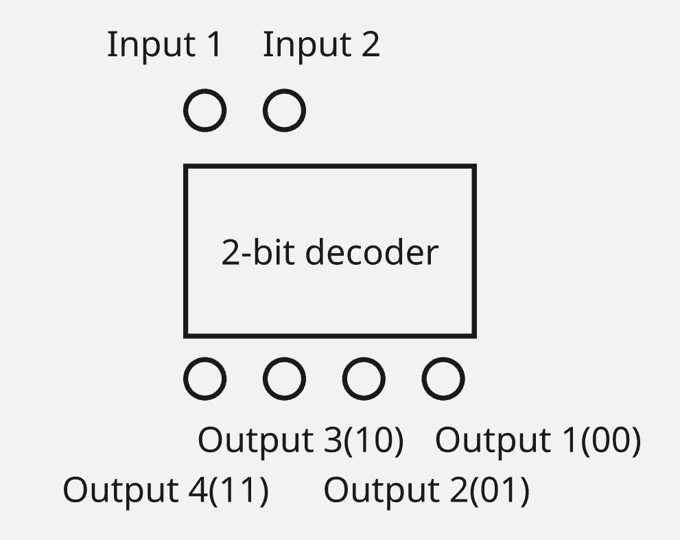
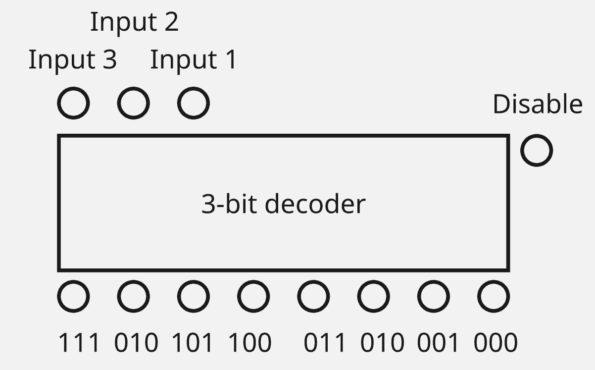
Goal 13: Decoders
The MUX can encode which out of inputs should be selected. Let’s now think about doing the (almost) inverse. We will need to be able to map a state of one or more bits to a single output. For example, if I have 2 inputs, I can represent 4 states. To be able to make decisions based on a state that is made up out of multiple bits we will need to write a decoder.
Let’s start small: With one bit we can have two states. So we need two outputs. One will need to be one when all others (in this case only one other) is off. The NOT-Gate comes to mind:
This is the simplest 1-bit decoder that I can think of. It demonstrates nicely what we want. One state of the input relates to one output outputting one and the rest zero. Now let’s make it a bit larger and do two bits. With two bits we can have 4 states. The truth table that we would like is the following:
Decimal input state index
Input 1
Input 2
Output 1
Output 2
Output 3
Output 4
1
0
0
0
0
0
1
2
0
1
0
0
1
0
3
1
0
0
1
0
0
4
1
1
1
0
0
0
From the above 1-bit decoder, I can see a combinatorial problem here. We will need an inverted and non-inverted wire for each input. This gives us 4 wires. We then need to combine each pair of two in some way and pass that to the respective output.
But how to combine each pair of these? We want to only give an input if there is a unique state (e.g., 01) across all inputs. Let’s try to think about state 00 first and maybe we will get an idea. For this state, we need to have both inputs 1 or equivalently both inverted inputs off. Either of the two will do. We can test if both inputs are on using the AND-gate as we did before. Similarly with the 11 state but inverted.
I hope it becomes clear now what I was talking about when I said that I see a combinatorial problem. Concerning the last two inputs, we just map the second two to their respective states.
We will use represent this circuit in a simplified for later:
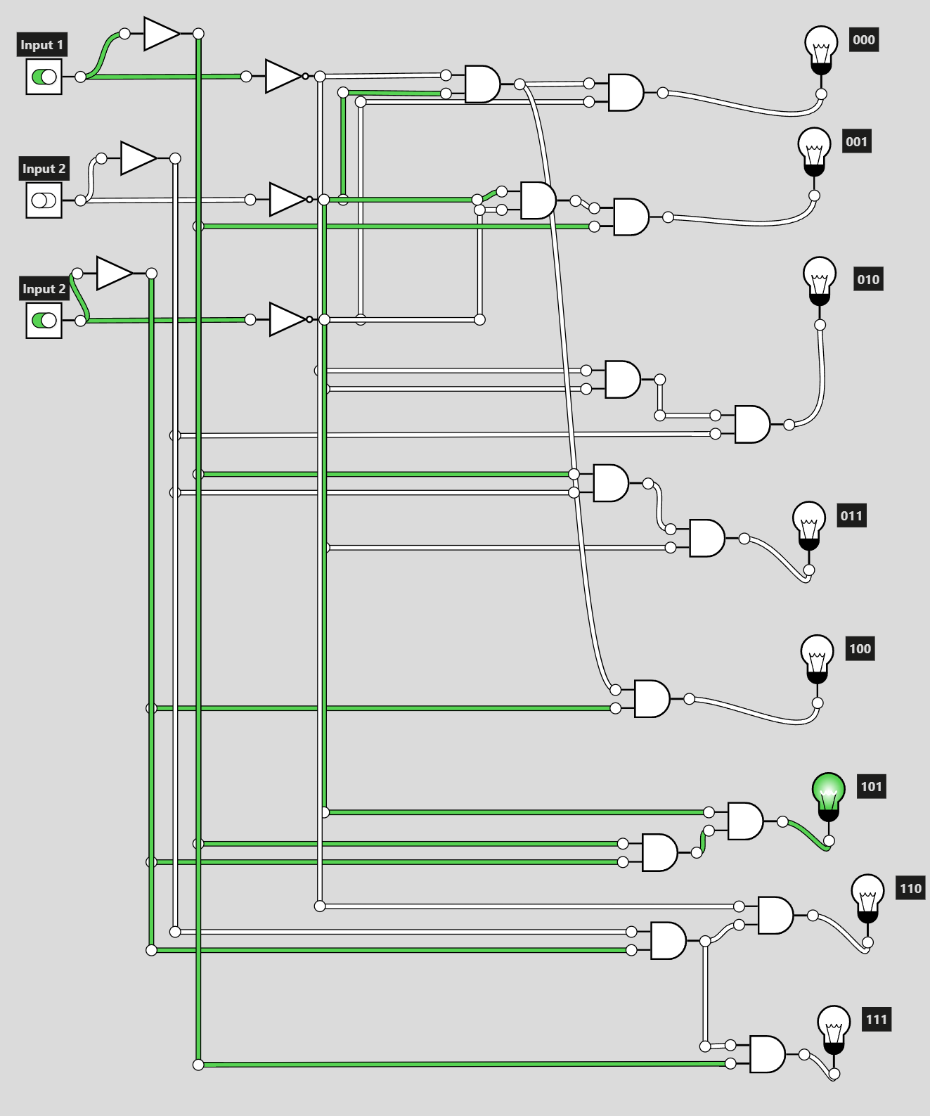
For a larger decoder, we can simply extend the design downwards. Here a 3-bit version:
You may be able to notice that some of the AND-gates can be used multiple times.
For example, here the 001 state and the 101 state both share the left most state. You can see that we would have been able to save 1 AND-gate in the second row (where 001 is being decoded). We will need this decoder to make sense of multiple inputs and control what our computer will do. Again, we wrap this into a simplified representation for later:
I was sneaky and added a “disable” input as well, which is just another layer of AND-gates with the inverted “disable” input. When the input is turned on, the decoder will be disabled and all outputs will be 0. We will need this in our computer later.
Goal 14: Saving 1 bit
By now we understand binary inputs as numbers, have a way of selecting inputs and do some arithmetic on these numbers. However, we have now way of storing our inputs and outputs yet. We will definitely need to be able to store intermediate results if we want to do more complex calculations. The alternative would be to always build a new circuit, but without a way to quickly assemble such a circuit on the fly, this does not seem feasible. Let’s start with a single bit.
So far, we have only looked at logic that did not depend on the order of previous operations. It never mattered what configuration of inputs came before the next. If we want to save a bit, we will need to change this, which we can do by connecting the output of a gate back into it.
This is nice, but we also need a way to reset this circuit back to the off state. Let’s try to add a second button and extend our design from above.
This circuit has the same problem. There is no way of turning the circuit off once it is in the on state. We need to invert the output of our OR-gates for this. As a reminder, here is the NOR-gate truth table:
Input 1
1
0
0
1
Input 2
0
1
0
1
Output
0
0
1
0
I rebuilt this circuit from above using NOR-gates. This works as we want. We can cycle through the sequential states of saving a state:
This gives us the following truth table for the SR-Latch:
1.
2.
3.
4.
Reset
0
0
1
1
Data
0
1
0
1
Output
nothing changes
Out = 1
Out = 0
Invalid state
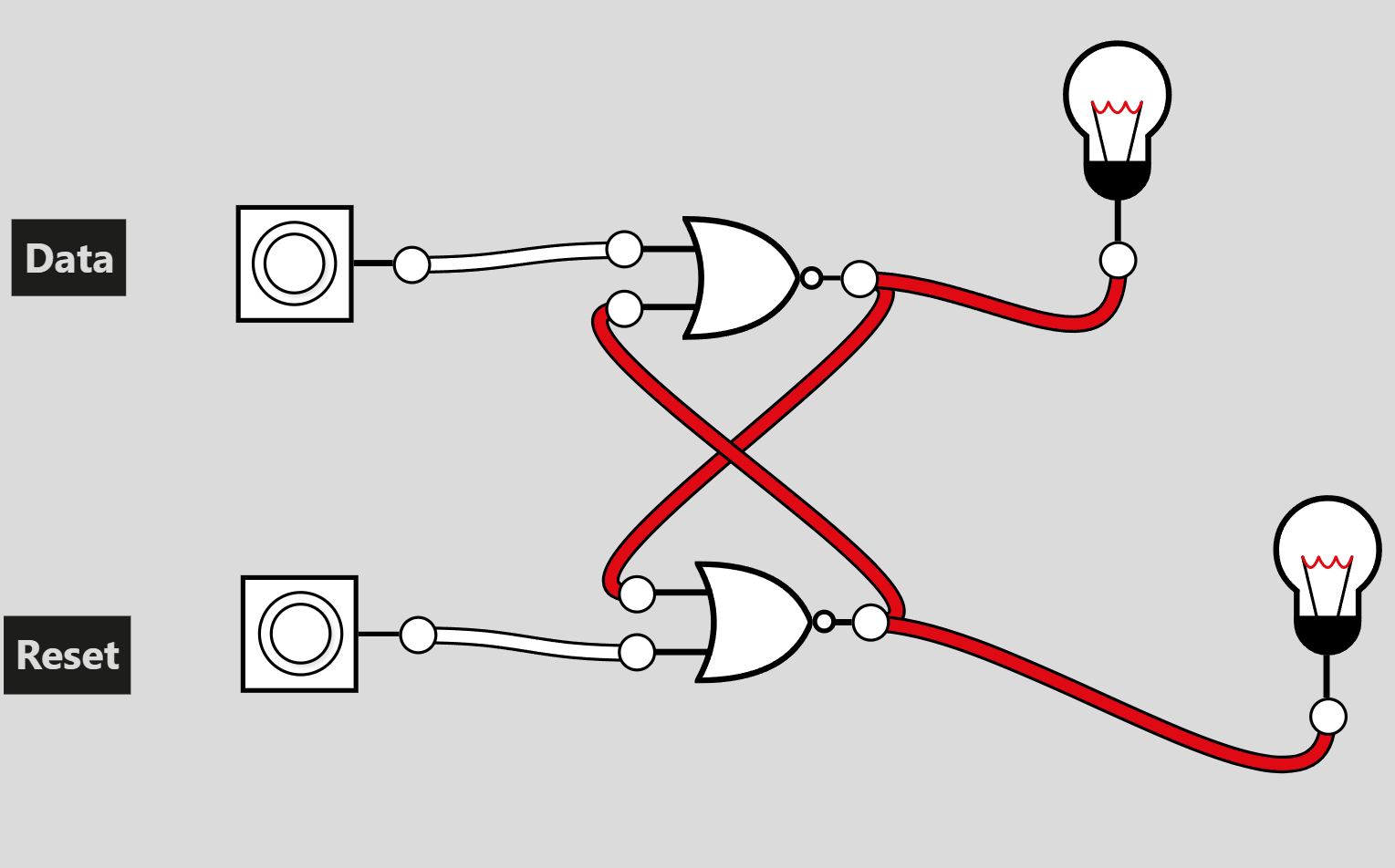
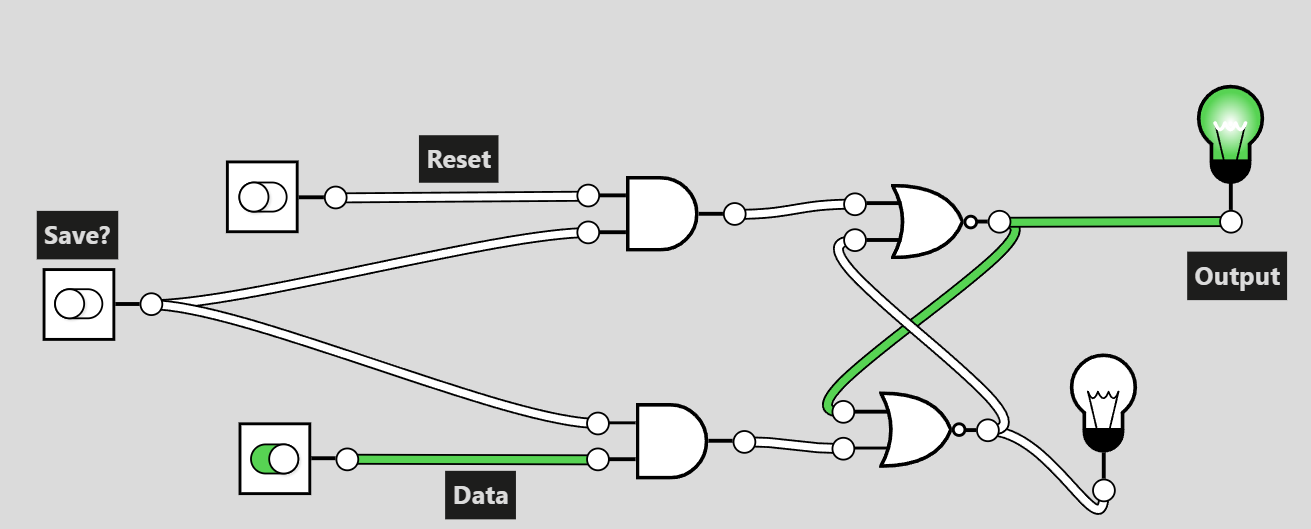
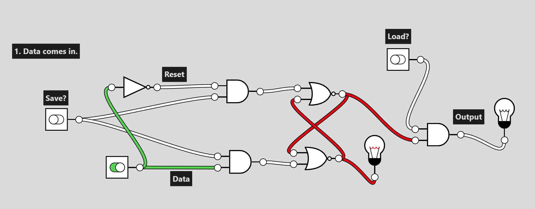
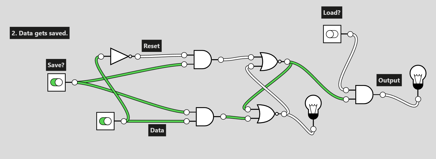
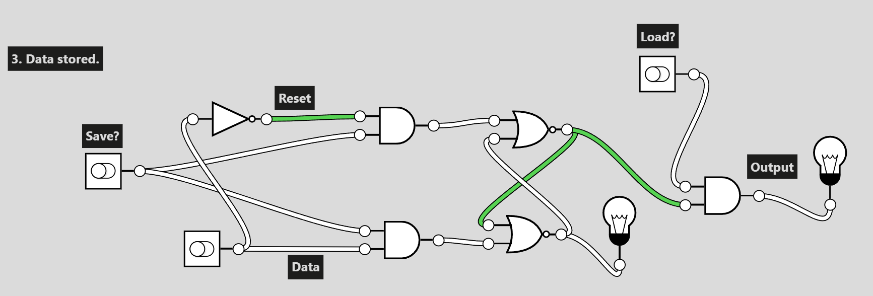
It does not make much sense to set both inputs to 1, because then would be telling our circuit two opposing things. This circuit is called the Set-Reset-Latch or simply SR-latch. Now let’s see if we can modify this input to be a bit more intuitive. I would like a single input and a “save” button. We could imagine that we have some state of a document for example, and then we would like to save that state.
So we want two things:
Single Save Button
Single Data input
If we look at the above truth table, we can reason about how we can make that happen. The “save” button should toggle between state 1 where nothing changes and states 2,3 where we can set the new value. We can start by implementing this “save” button using two AND-gates:
Gated S-R latch:
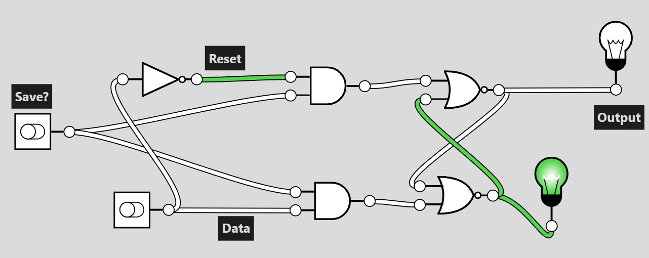
Now we are able to enable and disable the latch by using a third switch. This is nice, part 1 is done. We only need to get rid of the “reset” input now. Looking at the above truth table (again i know), we notice that when the latch is on, we can deduce the state of the Reset button from the state of the data. It is always inverted. If we were to feed the inverted data input to the reset input, we could easily accomplish the same! This also avoids us tapping into the invalid state where both reset and data are 1.
We arrive at the final result, the D-latch:
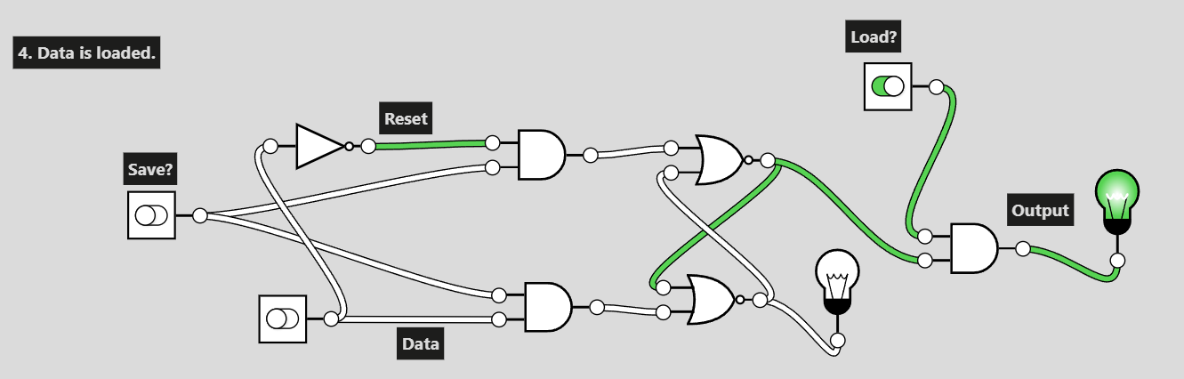
This is great! We can save the data stream just like we wanted when we press save. We could now also add a load condition that outputs the output to something when a third input is true the same way.
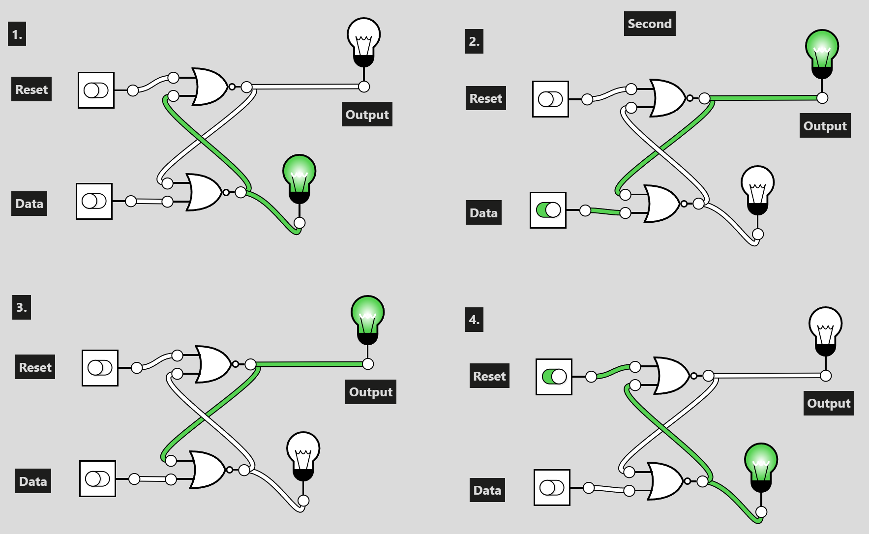
13.1: Saving more bits.
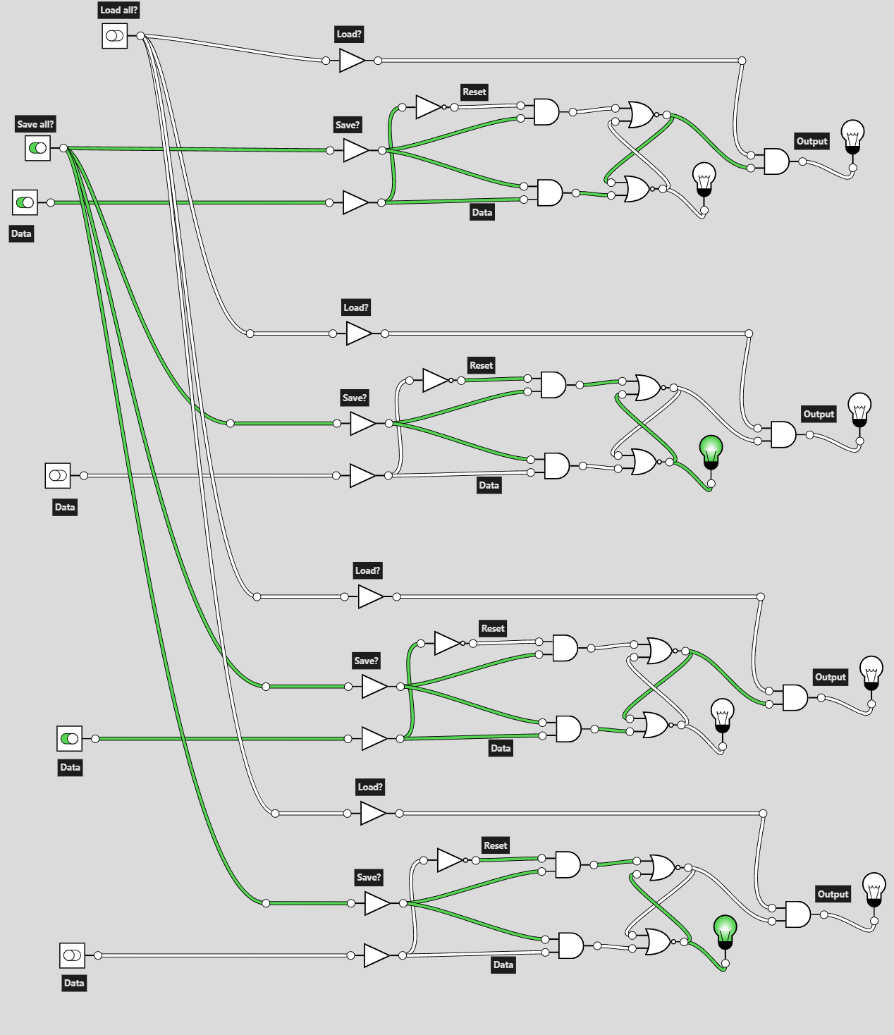
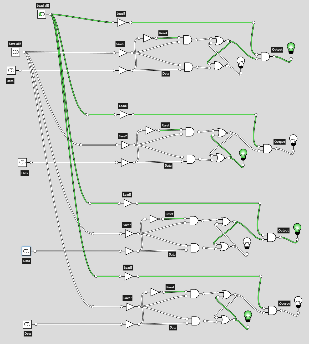
We can tile this just like we did with the 4-bit adder to save as many bits as we want:
And load the stored data:
Again, we can compartmentalize this logic in a block:
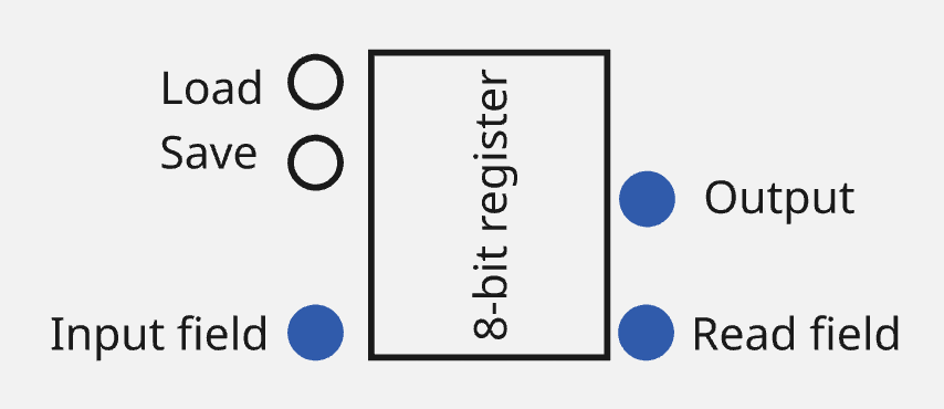
I have added a field for the output that will get the output only when load is on like above. However, maybe we want to have a second option and be able to just read the field at any time. For this, I have added a separate output that is only for reading the contents of the register. Again, blue circles refer to byte-wise input and outputs.
Goal 15: Defining instructions
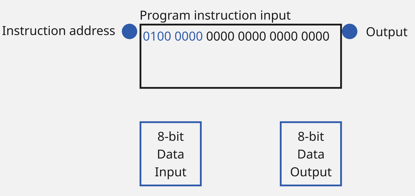
We would like our computer to be able to take in a list of instructions and give us some output. Let’s think about the instructions. If we want to pass in an instruction, we need to encode it in some input state. We know the circuits we build so far can only work with binary inputs, but generally are expandable as to how many input states there are inserted. Let’s limit ourselves to 8-bit instructions so that the task remains contained.
To do something with an instruction, it needs to have some meaning. Let’s select the two most significant bits to determine that meaning and the rest be the data.
If we think about what sort of things I would like to do with my computer, then I know I would like to take two numbers and combine them in some way and save the result. Just like with a calculator. There are obviously a bunch of other things I would like my computer to do, but these are the simplest that I can think of, given the logic that we have already implemented. We know that our computer will have to work with a set of binary inputs and we also know that these can be understood to be numbers. Now, the next logical step is to build from there and see that we are able to do operations on these numbers.
Let’s define the instructions that we want and encode them into the two bits we selected:
00
01
Do some calculation.
10
Copy a value.
11
I obviously left out two states, but bare with me for now. We will find some more interesting actions that we would like to assign to those states. For now, we know that we will need some registers to save values, something that can do calculations and something that decodes what the instruction means. We can start with just saving and copying values between registers.
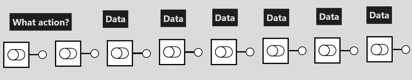
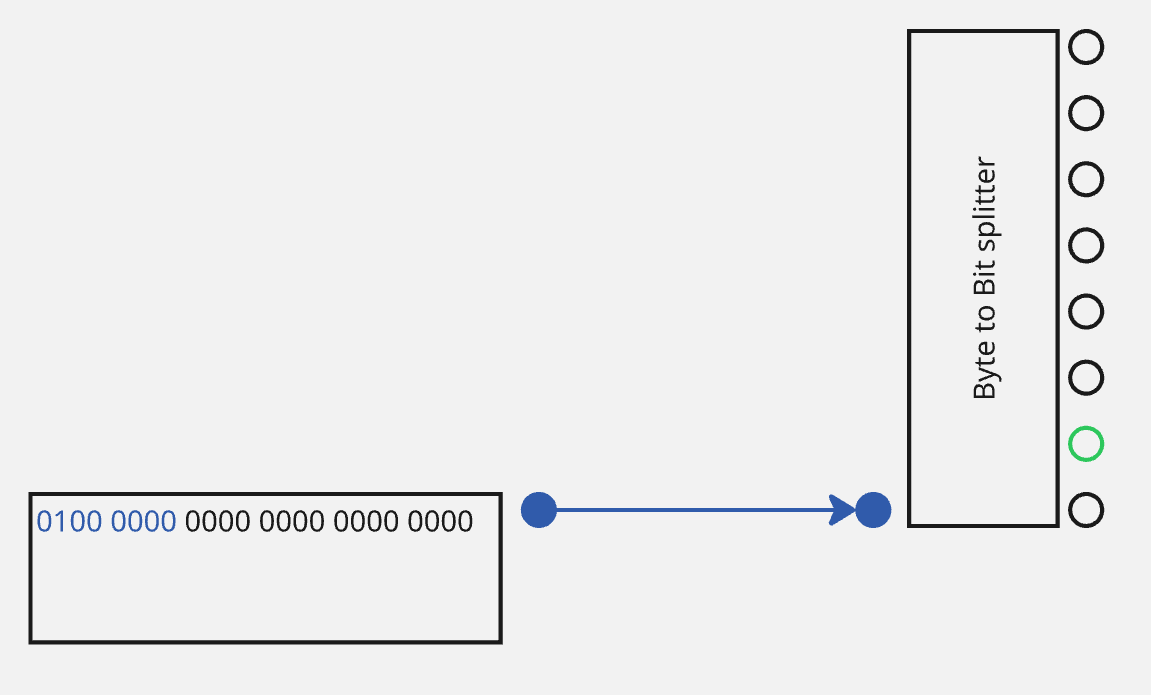
I have changed to a bit of a different representation to make it a bit less messy for us. Blue connections will be used to refer to BYTE transfer. A byte is 8 bits. We can imagine such a blue wire as just 8 different wires next to each other. Black wires are single bit wires and green wires are single bit wires with the 1 state. For example, the 8-bit version of the tri-state buffer we discussed before will look like this:
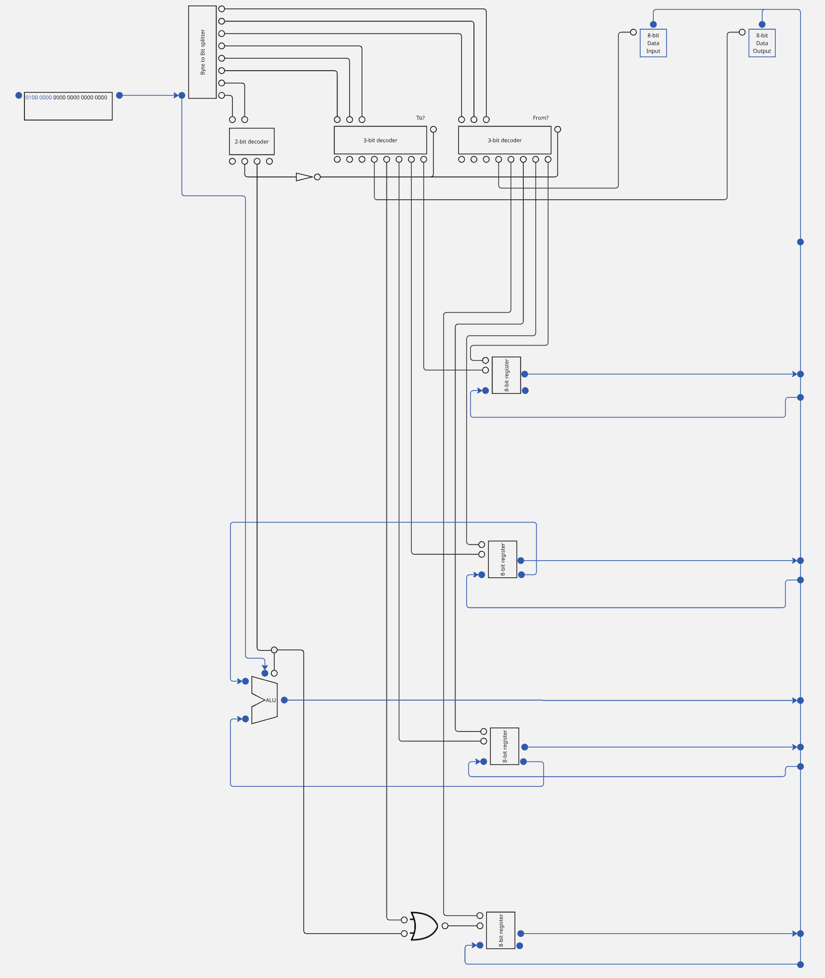
Now to our starting point. We expect that there will be some long string of 0s and 1s that encode the instruction. The instruction address takes a number as input that denotes the index of the byte that we have to read. The output just outputs the bytes. Secondly, we also have separate data input and output streams. These contain the numbers that we perform the operations on. We assume some hidden process here that will provide us with the right numbers at the right time. It could for example be that, much like the program instruction input, the data input just has a long list of numbers that is defined before and is then read into the program. Not very dynamic but good enough for now.
Goal 15.1 Copying values
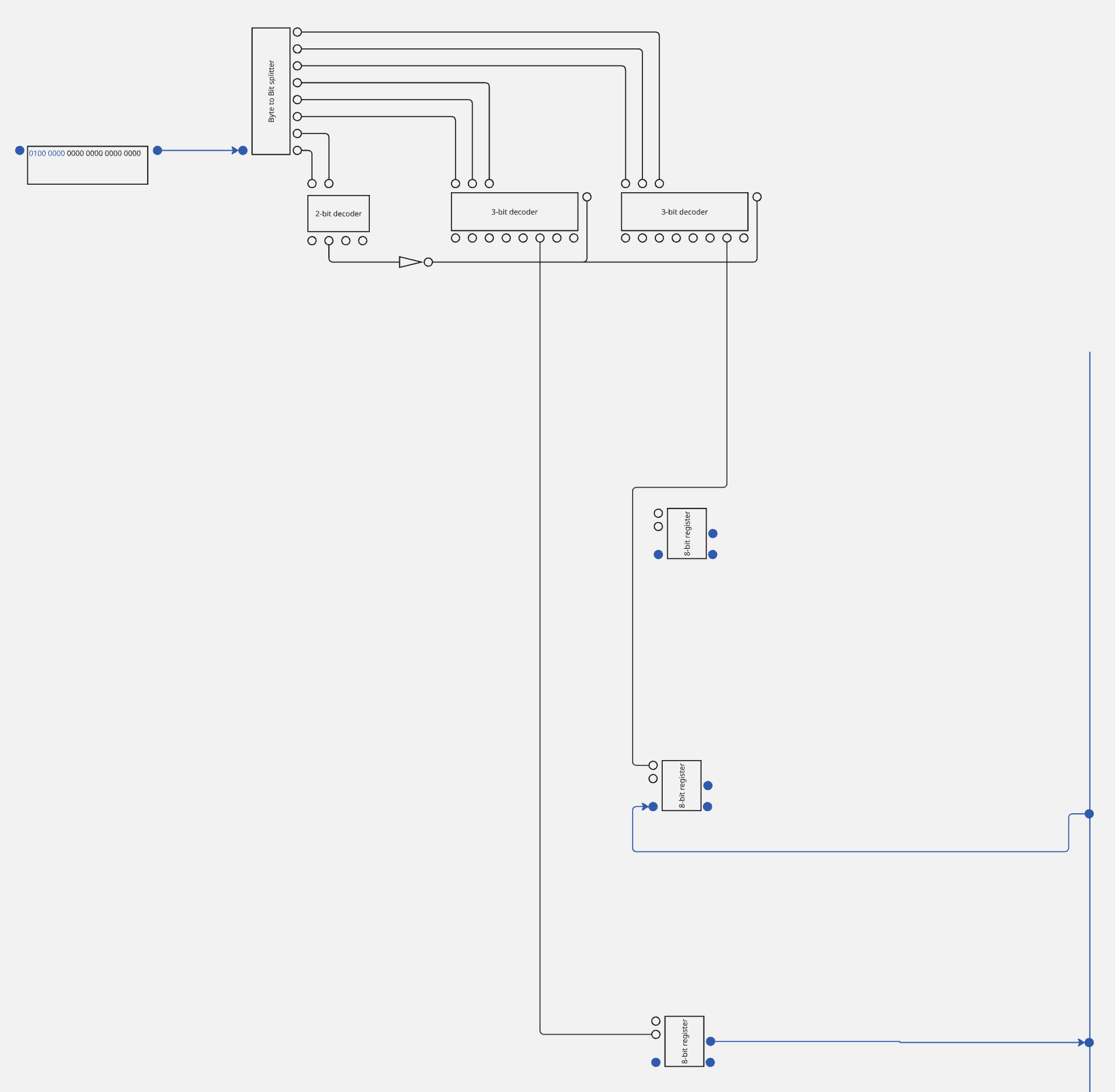
I will first decode the byte into its separate bits.
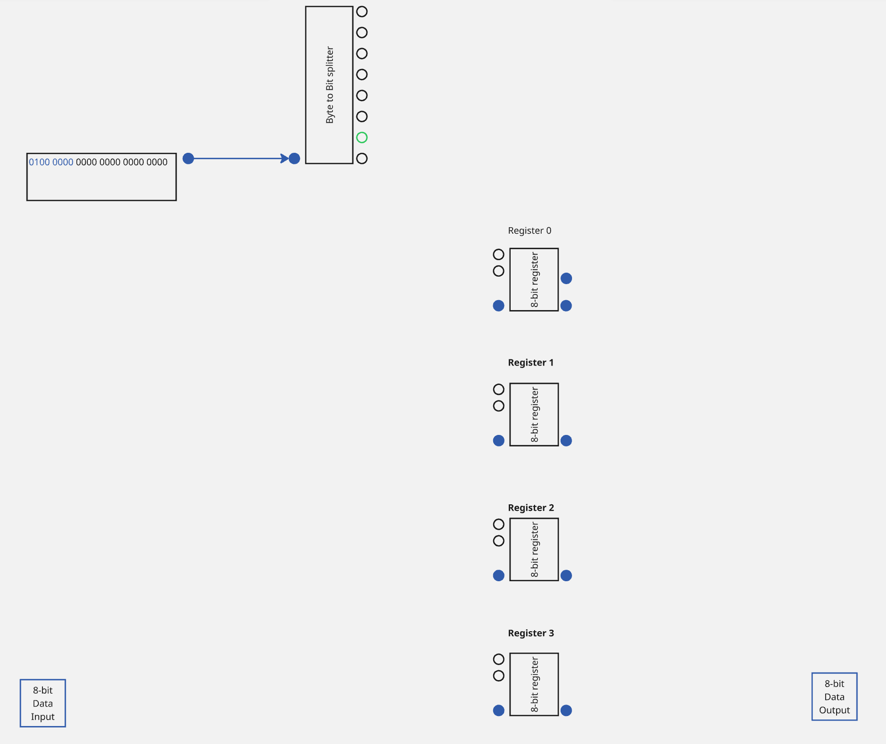
We want to be able to copy between two registers and an input stream and output stream. For this, we obviously need to have some registers, so I will add four to our architecture. Note, that this can be as many as we want.
We will need to define a set of instructions for the copy operation between registers and input and output. Let’s use this convention: Out of the 6 left-most bits in the instruction, we use the three most significant ones to determine the location to copy from and the three least significant ones to determine the location to copy to.
Decimal index
From
To
0
000
Register 0
Register 0
1
001
Register 1
Register 1
2
010
Register 2
Register 2
3
011
Register 3
Register 3
4
100
-
-
5
110
Data input
Data output
6
111
-
-
For example, I would like to copy a value from the input to the output. I know I will need to say “copy” by setting the two most significant bits to the state “01”: 01 000 000. Next, I know that the “from” field should be 110 and the “to” field should be “000”, because these map to the input and register 0 respectively. The correct instruction string then is 01 110 000.
In a second example, imagine we want to copy from register 2 to register 1. Again we know the prefix is “01” to indicate a copy instruction. Next, we need to look up the fields for the involved registers and come up with 01 010 001.
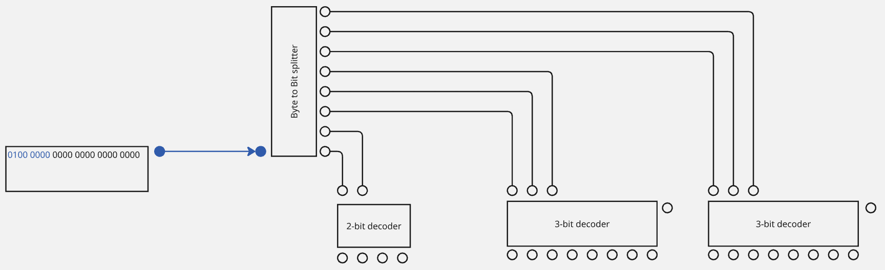
Let’s try to implement this logic. First, we need to decode all three sets of bits: the two bits indicating the action to be taken, the “copy from” and the “copy to”.
Let’s start with our second example. I would like to copy a value from register 2 to register 1: 01 010 001. For this, I will need to do three things:
Connect the output of register 2 to the input of register 1
Enable both decoders
Set the “load” and “read” fields of the respective registers.
Doing this for registers, as well as the input and output, completes the copy implementation.
Let’s move on to the second part of the logic we wanted to implement: Computation.
Goal 16: Arithmetic and Logic Engine (ALU)
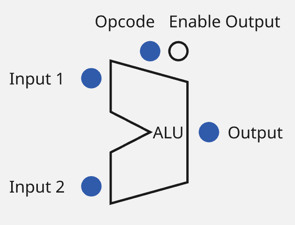
It would be useful to integrate all the operations that we have learned to implement so far into a single block. We could then pass the data as well as a selection input to the block and let it spit out the result. This block could be split up into two parts: One that does all the logic operations (or, nand, nor, and) and one that does all arithmetic (addition) operations. This time, let’s start with the abstract representation. There should be two inputs and one output. Additionally, there should be one input that decides the operation we would like to have:
The “opcode” field decides which operation we would like to do. Let’s associate some numbers to the operations:
Opcode
Binary Opcode
Operation
0
001
OR
1
010
NAND
2
011
NOR
3
100
AND
4
101
ADD
5
110
SUBTRACT
We should add this to our instruction as well. We can use the three least significant bits of our instruction to encode the type of computation when the most significant bit are set to the “computation mode” (01) as such:
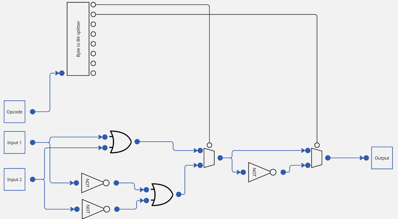
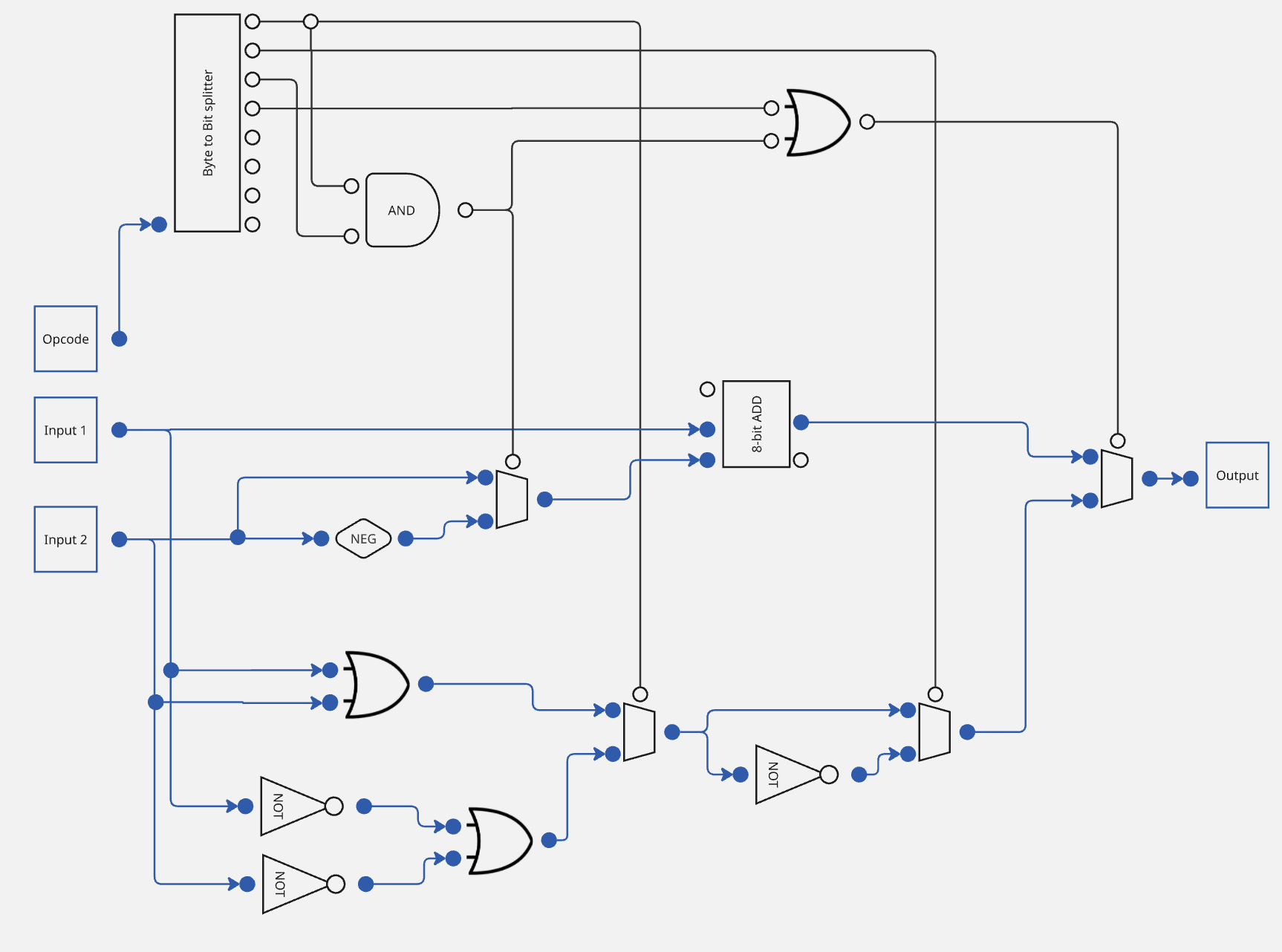
For this exercise, I will be using the byte variants of the basic logic gates to make the illustration a bit clearer. These can simply be understood as doing the operation of the gate for each input bit. Following De Morgan’s laws from earlier, we know that the operations we want are all related and can be encoded in terms of one of the gates in the diagram combined with inversion of input or output. We can use the multiplexer (MUX) from before to decide which combination should take place: Should the input be inverted? Should the output be inverted? We are left with the circuit for the “logic” part of the ALU.
Now we need to implement addition and subtraction. We know that subtraction is just the same as addition of a number with a negative number. We can use the negator we discovered earlier to invert the second number and pass that to our 8-bit adder.
You may notice that I added an extra AND- and OR-gate to select the input of the MUX. Naturally, we could have used the decoder we built earlier instead of decoding the state with those two gates.
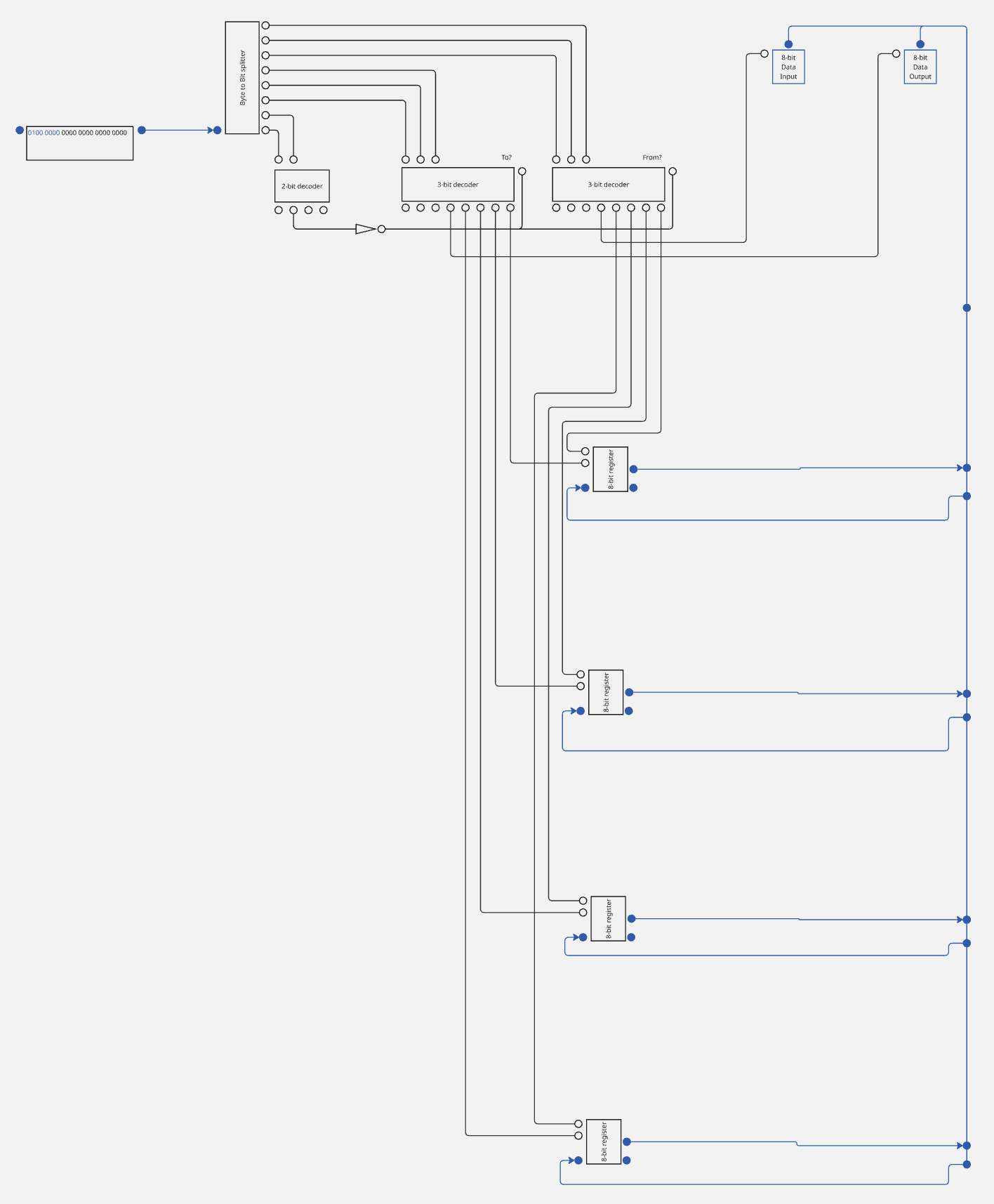
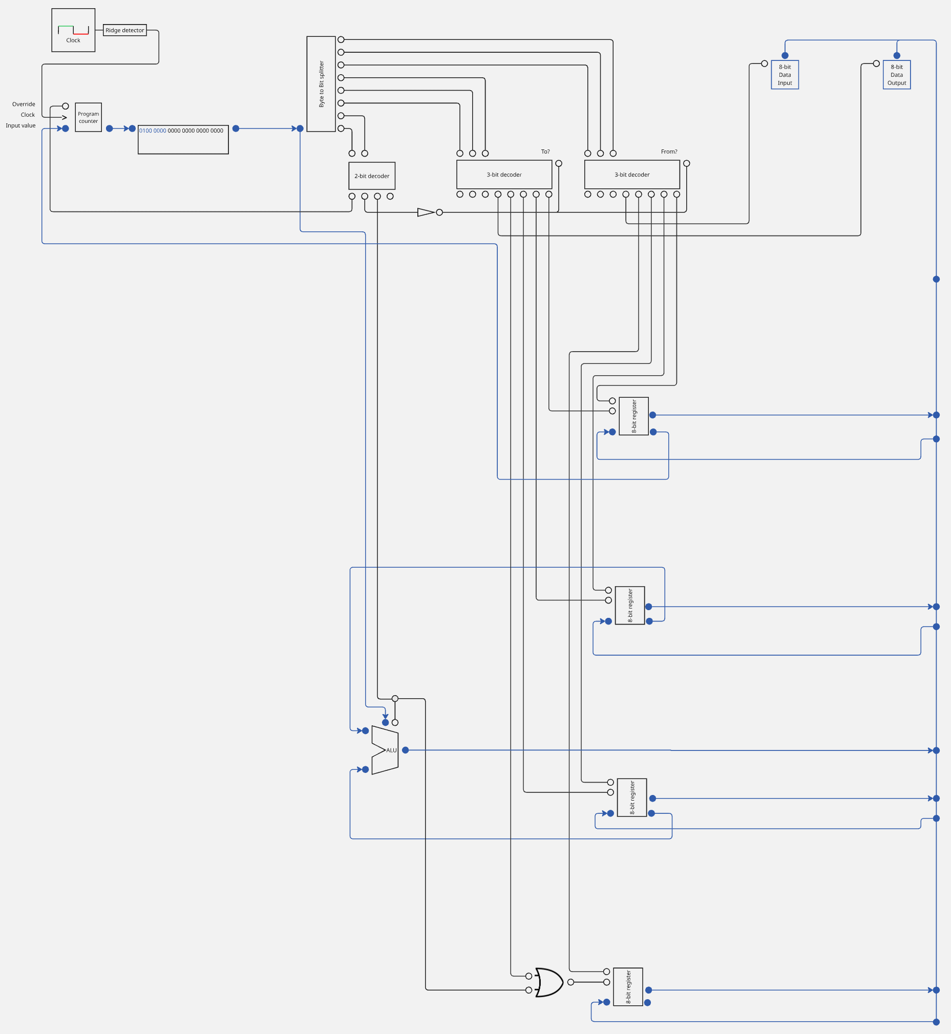
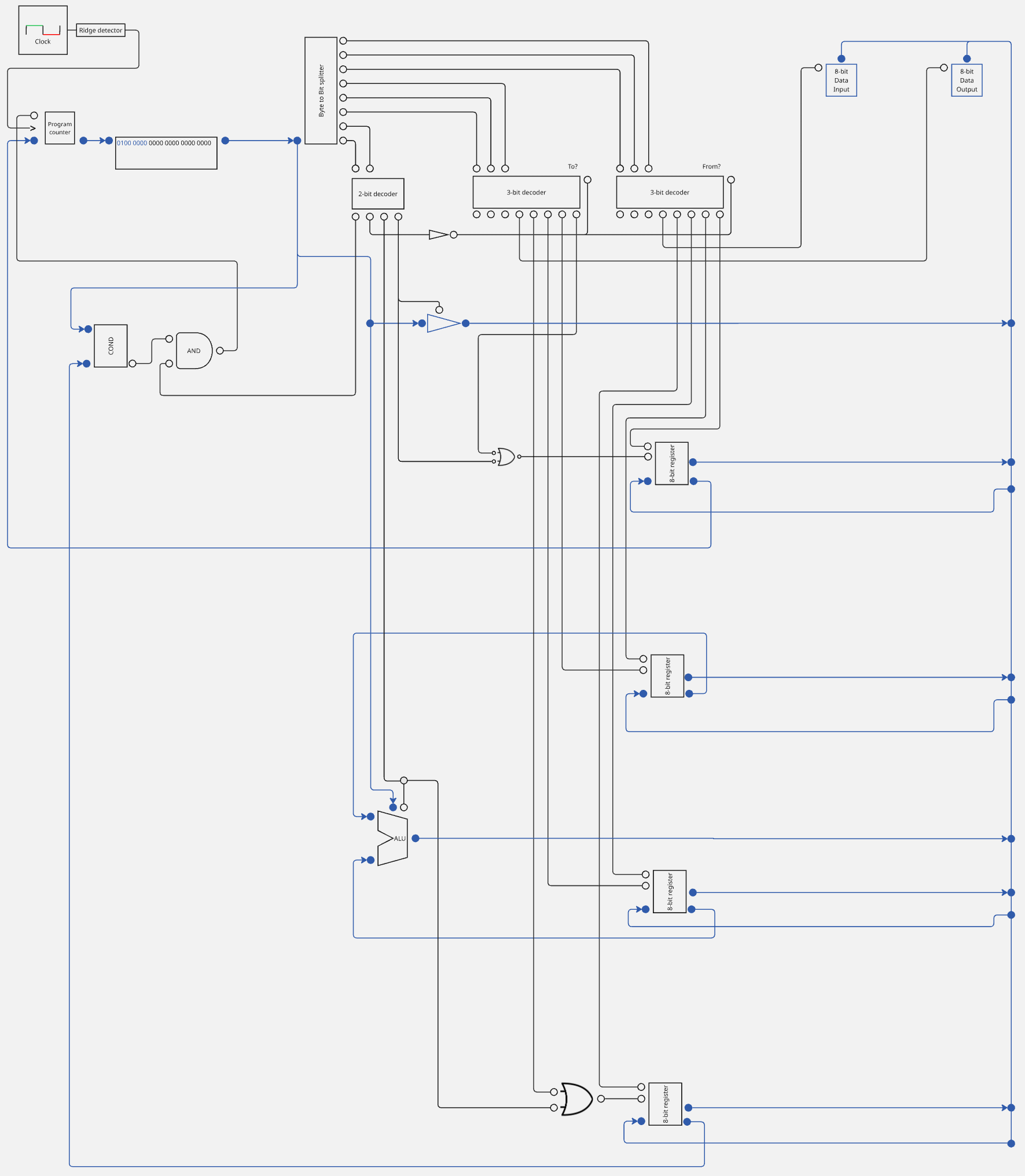
Next, we can wire up the ALU to do computations between fixed registers. Here we stand before the decision as to which registers to do the computation with. We could add additional logic to our instruction code to determine the registers, but do not have enough bits. I chose to just fix the registers that we can do the computations with. This effectively forces the programmer to move the to-be-computed data into the correct registers before the computation. We could do better, but this does not limit the amount of possible computations in any way, but computation may take more operations. I determine that computations must happen with Input 1 coming from register 1, input 2 from register 2 and output is loaded into register 3. Lastly, let’s add an 8-bit tri-state buffer to enable and disable the module.
Let’s add the circuit to our computer. For this, we need to make sure to enable when in use and also add an extra OR-gate for the load operation on Register 3, since now there are multiple ways of loading a value into this register.
Goal 16: Program Counter
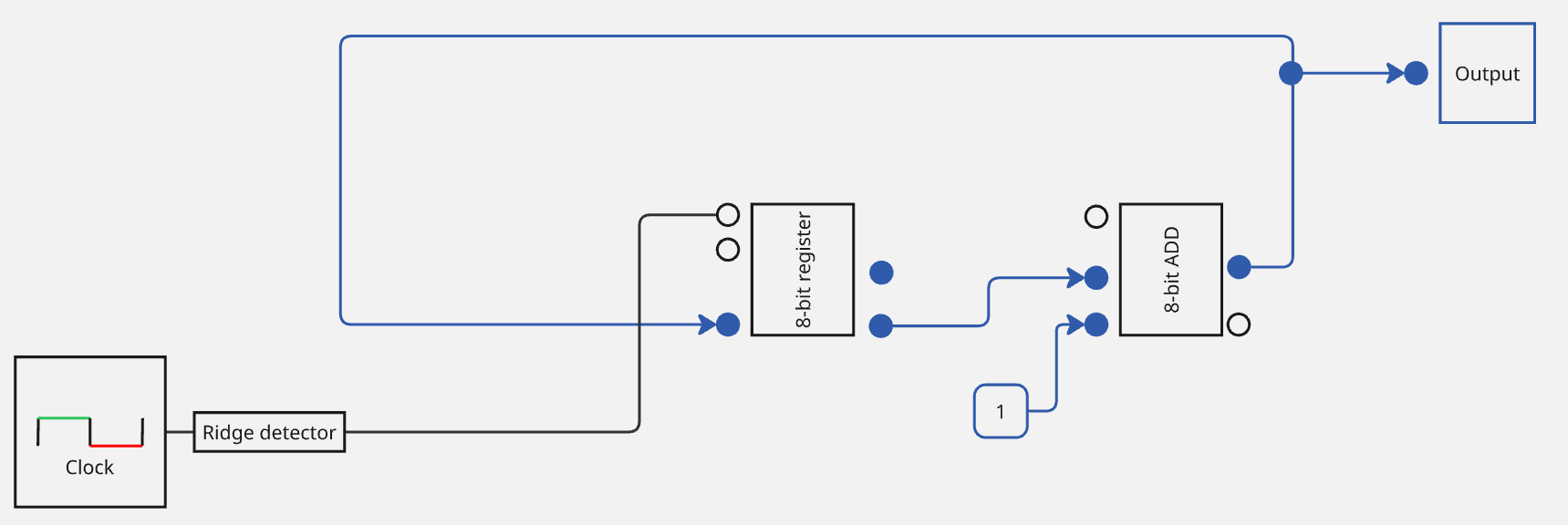
When we set out to build this computer, we decided that the input should come as one large string of bits, with us selecting 8 at the time and forwarding these to the splitter. However, we need to provide an index of which 8-bit block to select and forward. Currently, there is no input to the program block, so we will always be reading the first index. We should think about what we want. When I read a recipe, the instructions are provided in order: 1. Boil water 2. Clean potato. 3. Peel potato, etc. The index increments by one with every completed step, just like a counter would. We need one!
For a counter, we will need to store data. Let’s start with a known building block from when we built our 1-bit register in chapter 14: the SR-latch.
Previously, we then extended to this intermediate representation with an “enable” input.
with the associated truth table:
Enable
1
1
1
1
0
Reset
0
0
1
1
any
Data
0
1
0
1
any
Output
nothing changes
Out = 1
Out = 0
Invalid state
nothing changes
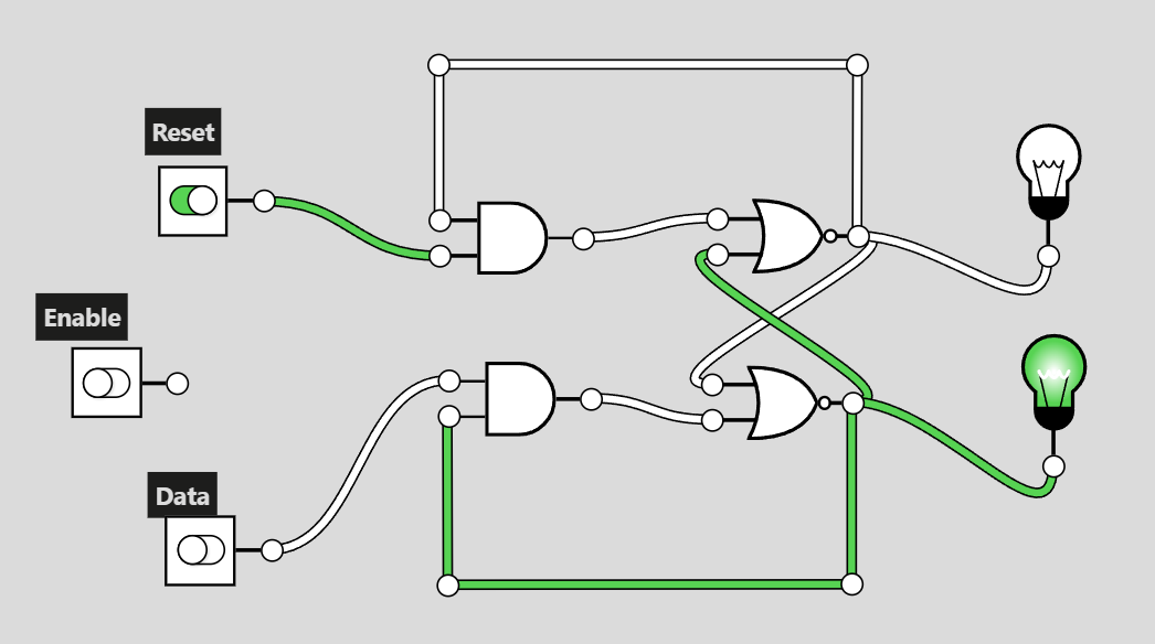
We went on to replace the “reset” button with the inversion of the data input to form the D-latch. This time, we won’t do that and introduce something else instead. The problem with the S-R-Latch was that we could hit an invalid state when all three inputs are one. In this case, we are telling the latch to latch high (1) and latch low (reset, 0) at the same time. This leads to race between both inputs to determine the output - not ideal to say the least. We can think about what this state should encode from looking at the above truth table. We have a way to do nothing, set output 1, set output 2, but no way to do the opposite of doing nothing: doing whatever action possible that would change the state of the system, a toggle between states. We can implement this by chaining another AND-gate behind the existing AND-gates and feed back the output of the opposing side. As it turns out, this preserves the logic of the SR-latch but adds the wanted behavior for the 11 state:
Unfortunately, if we leave the enable input there out, the latch will jump back and forth between the two states. This is not good. We will need an element that gives us a strong but also very brief charge increase from state 0 to 1 back to 0. Turns out this is where the clock of the computer comes in. The clock will do something very simple, it will continuously flip the switch for us.
16.1 Clock
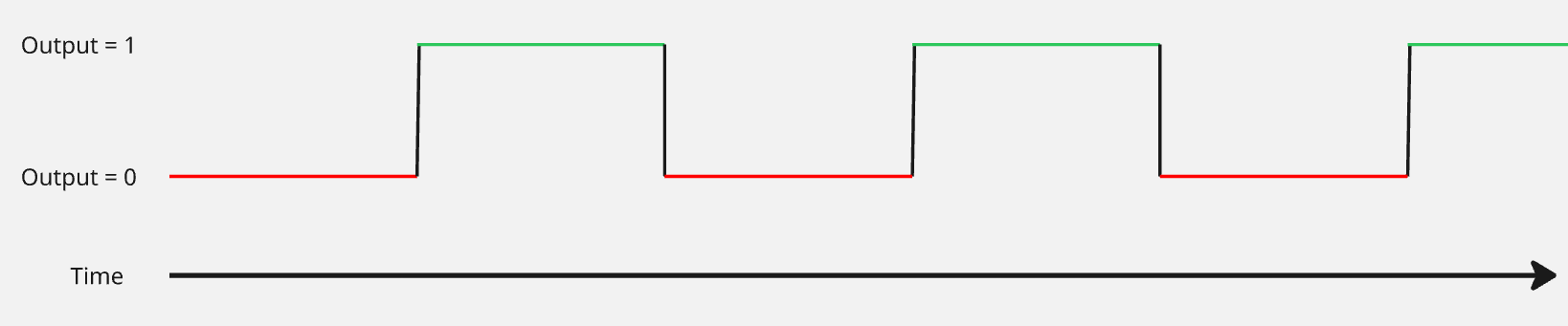
Over time, the clock we just thought of will be flipping between the two states 0 and 1.
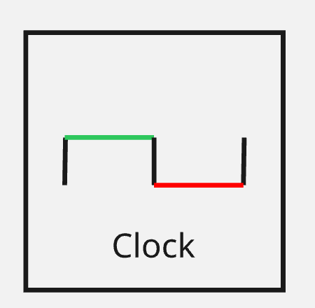
I would like to add a bit more nuance here. Technically, the states 0 and 1 do not exist in the way I drew them out but represent a difference in voltage. The clock continuously flips between high and low voltage states, creating the pattern we observe above. The associated symbol is:
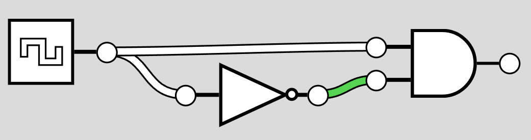
You may now wonder how this is helpful at all to us, since the phase for each state is still long. For this, we will add a circuit behind the clock that looks like this:
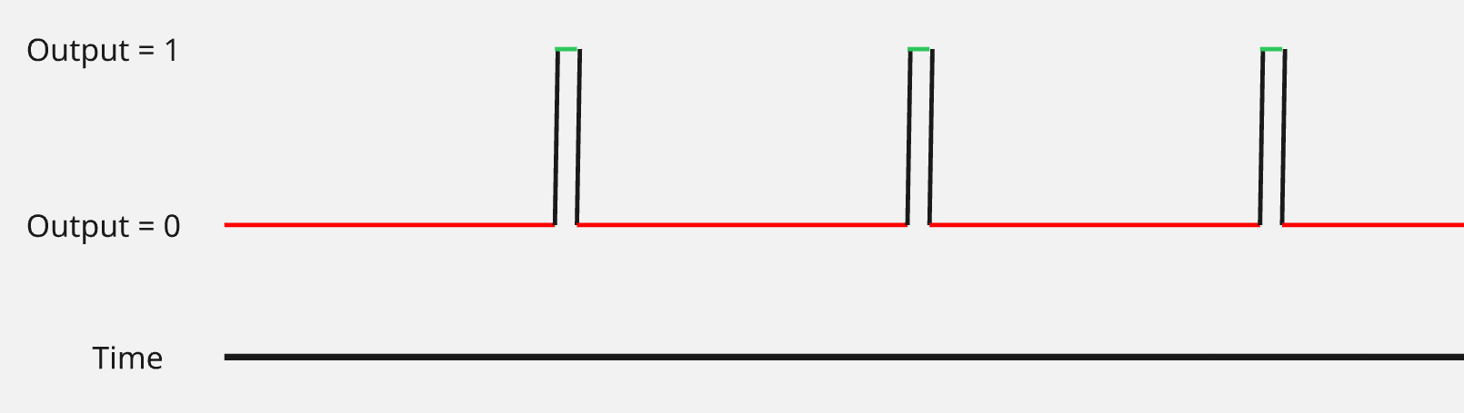
We know that each component is built up of transistors. These can only almost instantaneously pass on the signal, but there is a small delay. In this case, it takes the signal longer to pass through the NOT-gate than through the unobstructed wire. When the clock switches from low to high, for a very brief moment, both inputs to the AND-gate are high and the AND-gate forwards this. We have built a method to detect low-to-high cycle changes, a rising edge detector. We will use the combination of clock and rising edge detector to pass the signal through our computer. The output of this combination gives us the following waveform.
A short note on clock speed. Before this chapter, we have always assumed that the signal passes instantly. However, as we know now, each component has a cost of time associated with them. The computer that we are building has components that are very complex and need the signal to pass through others first. Take the Ripple-carry-adder for example. There, we can only start adding the next larger bit when the previous position is finished. In practice, this means that we would need to have a slower clock speed for our computer to ensure that all computation paths can be passed in a single cycle. This is particularly bad if the operation we want does not take very long at all, but since the clock is stepping ahead at a constant speed, we have to wait. Which raises an interesting challenge where we try to find ways to avoid waiting for previous components and move onto the next computation sooner, being able to increase the clock speed of the computer and its computation speed. I also find it interesting to think about the alternative, where we may not try to do a full computation in one cycle. Instead, we could try to break it up into smaller operations such that a single operation may take multiple cycles. This would have no impact on larger operations in terms of time, but since we know that the longest an operation could possibly need in the computer is much shorter, we are able to increase the clock speed. Lastly, if the computer has some means of predicting how long an operation may take, it would be able to adjust the clock speed dynamically, while still guaranteeing correctness of output. In our computer, we will put all of that aside and just use a slow enough clock speed.
16.2 J-K-flip flop & Ripple counter
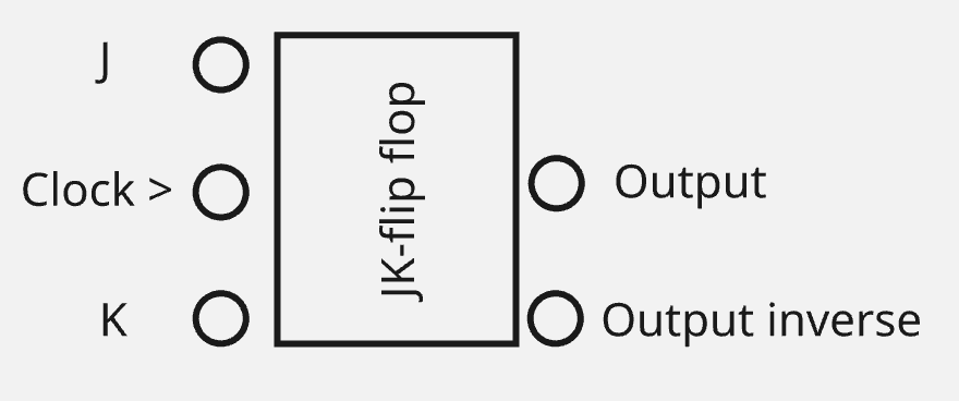
We can now complete our circuit called the J-K-flip flop from before:
Which has the associated truth table:
Clock/ enable
1
1
1
1
0
Reset
0
0
1
1
any
Data
0
1
0
1
any
Output
nothing changes
Out = 1
Out = 0
toggle
nothing changes
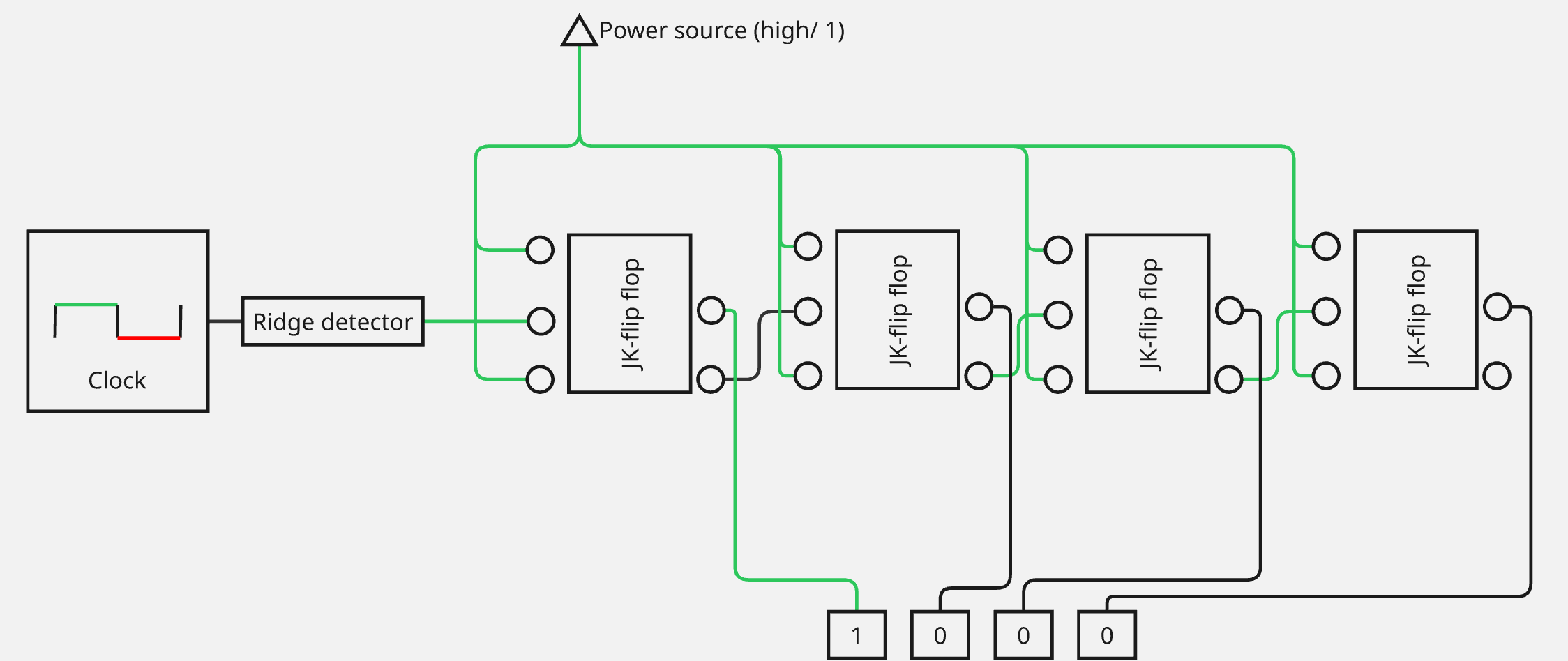
We can wrap this circuit into modules again as such,
and combine into a counter. In this counter, we use the inverted output of the JK-flip flop as the clock signal for the next flip-flop. Going from left to right, each clock signal will toggle the first JK-flip flop between outputs 0 and 1. The inverted output will obviously be the other binary digit. This makes it so that the next JK-flip flop will flip only when the inverted input is 1. This happens every other pulse. A falling edge/ transition from 1 to 0 will not trigger a toggle of the next flip-flop. The third flip flop will be dependent on the one before, etc. This leads the nth JK-flip flop to be toggled after flips of the first flip-flop. Effectively counting up. Also note how the output of this counter has the most significant bit on the farthest to the right position.
Similar to our ripple-carry adder design, the computation speed of this ripple counter increases linearly with the number of digits in the counter. There are fun ways to improve this, but let’s not get too sidetracked. Instead, we should think about what we do if we want to do more than just move to the next instruction.
16.3 Condition instruction
If we want to repeat the same operation multiple times in our current design, we would need to provide it multiple times to the instruction set. This is not only very dumb, bloats the program, but also restricts some of the operations that we can do. Branching is completely impossible. That is, if we want different instructions to be executed based on the result of previous computation or we cannot do this. We should, therefore, add a “condition” instruction to our instruction set:
00
01
Do some calculation.
10
Copy a value.
11
Condition
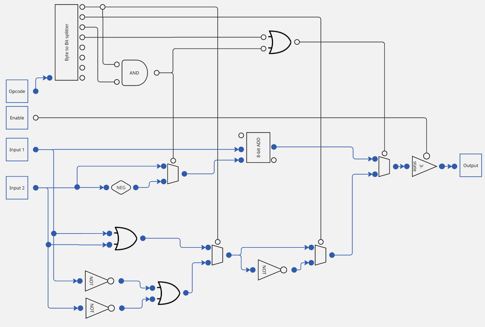
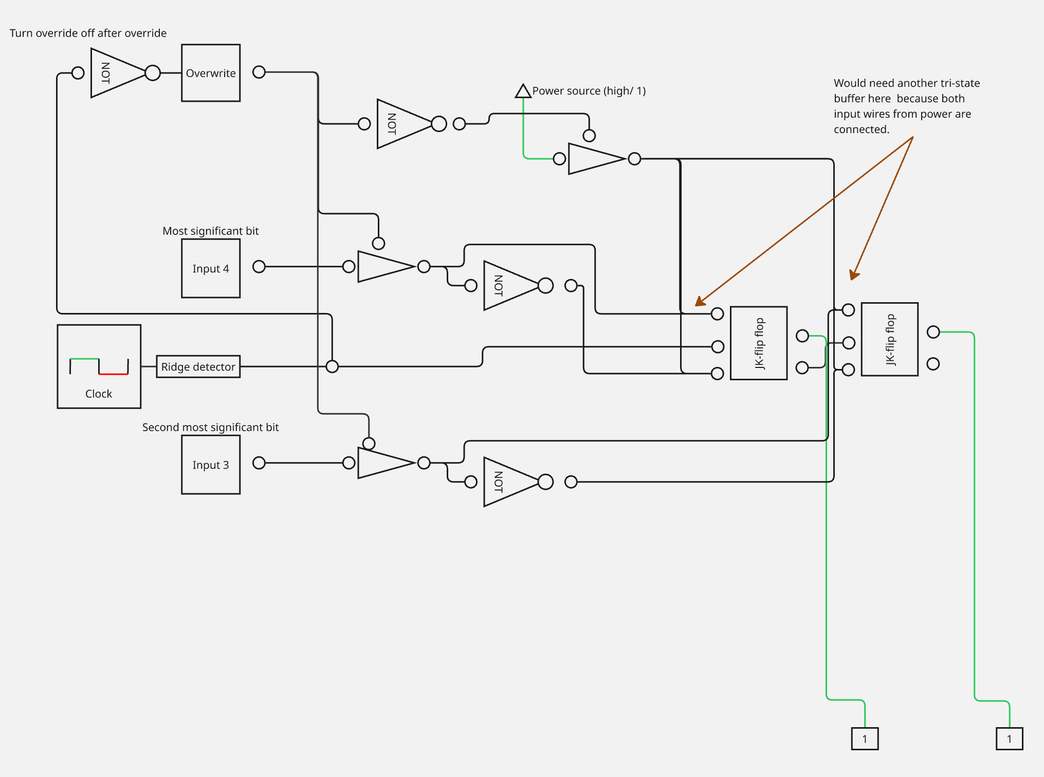
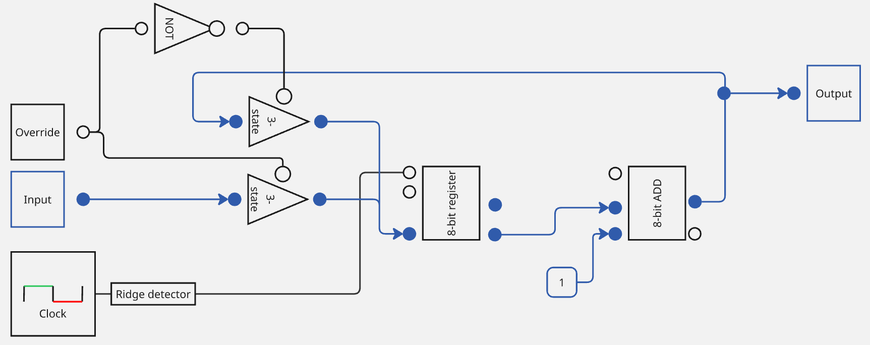
We know two things will be needed to implement this: First, a block that decides on the new position to be passed with associated instructions. Secondly, we need to be able to override the counter with the new value. After that, it should continue counting from that new value onwards. We need a “set value” button.
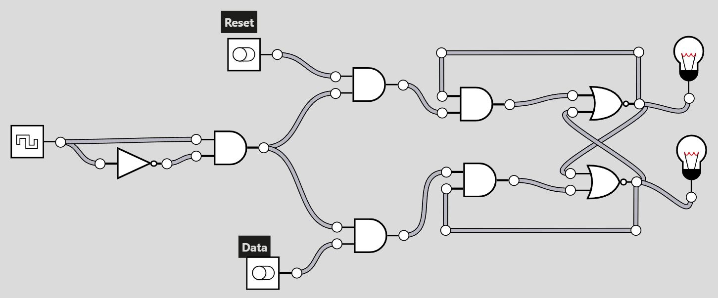
Seeing we are currently working on the program counter anyway, let’s avoid shifting focus and start with the second problem. For this we can try to add a second control path to our counter. For example, to set a flip-flop to 1, feed J = 1 and K = 0 when Load is active. Similarly, to set it to 0, feed J = 0 and K = 1. Since we will be sharing the inputs, we need to make sure to not short circuit the whole thing. I have created a two bit version of the design we would need below.
But since I am the one writing this text, I can do whatever I want - and I want something a bit simpler. Let’s take a step back and evaluate what we need.
Increment with every clock cycle
Storing input bits.
Returning input bits.
Now, painfully obvious, we could have accommodated the second two requirements with our 8-bit register from earlier. Incrementing is just adding by 1 and we have also designed an adder before. Can introduce the clock by just using the gated S-R latch from 13.1 and replacing the enable input with the clock.
Counter V2:
Much simpler to read for me. Adding the enable logic is almost trivial now compared to designing an entirely new circuit, because there is only a single input loop that we need to protect with tri-state buffers.
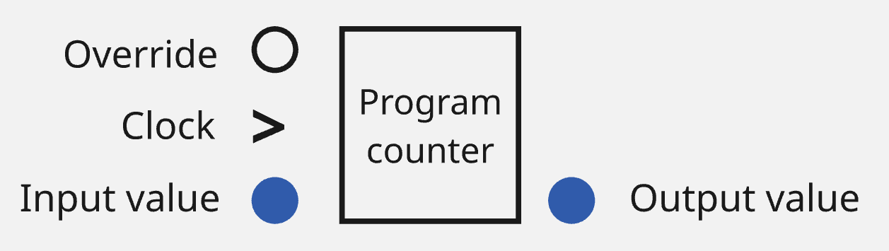
I am very happy about this! Let’s make it a module and wire it up to the rest of the computer:
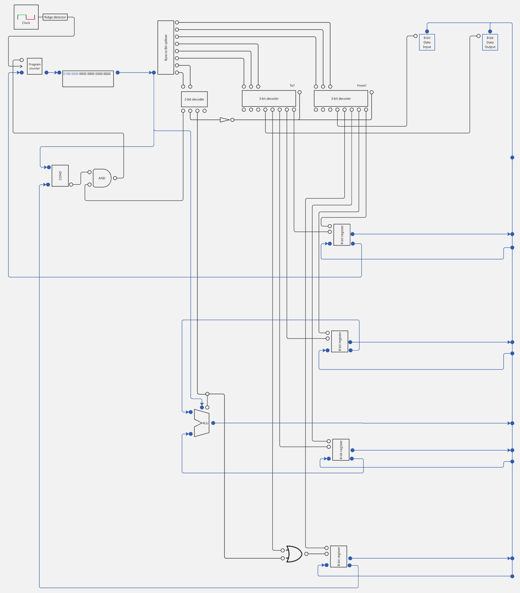
Similar to when we implemented calculations with the ALU, I made the decision that the input override value can only come from a specific register. This time, I chose Register 0. Notably, we are still missing the block that makes the override dependent on the data. In the current setup, the condition instruction would always override the counter value with the value in register 0. Let’s have a look at that next.
Goal 17: Condition Engine
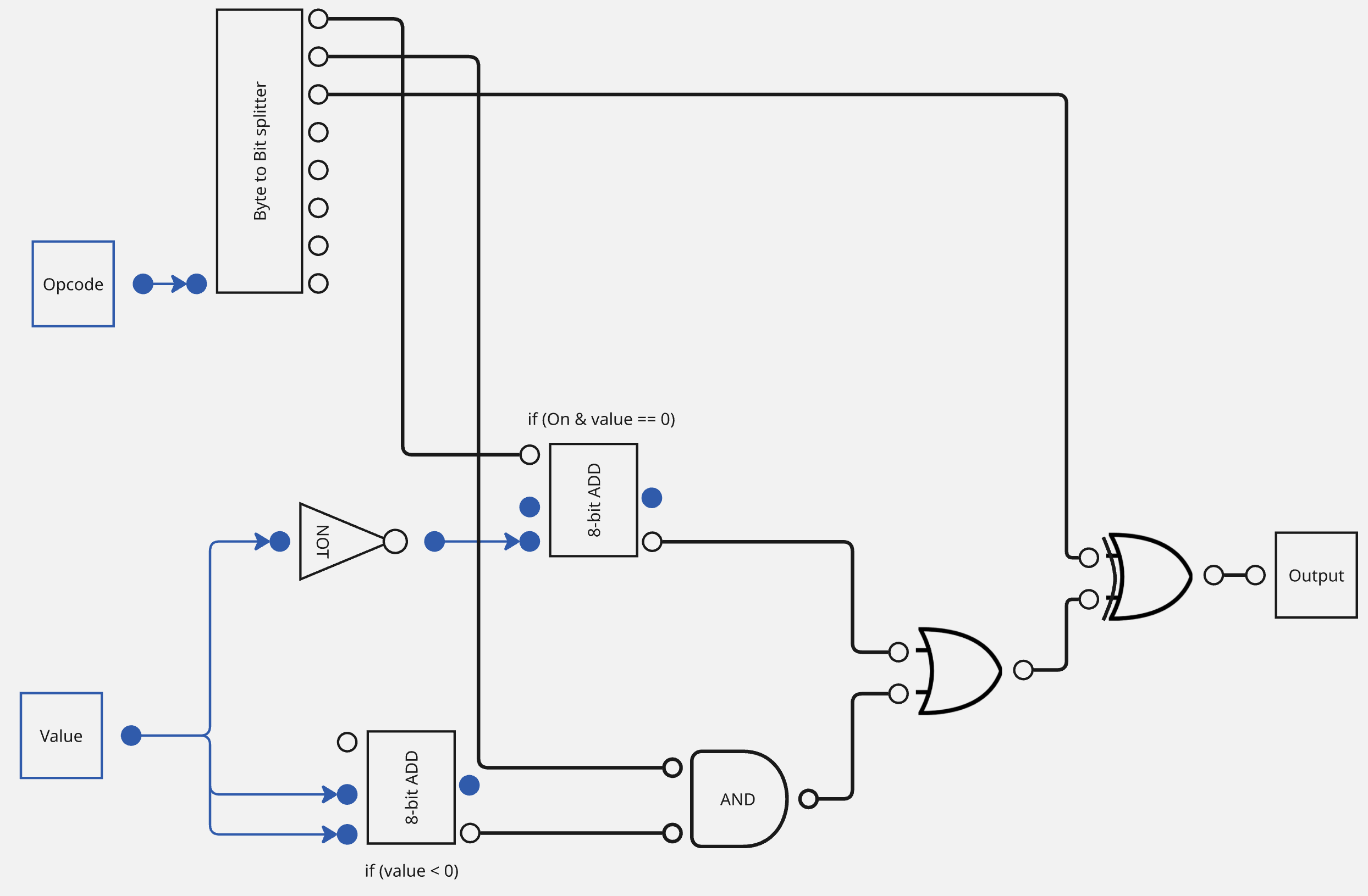
When the instruction code is 11, we decided that conditional branching should happen. This means we need to compare two values. For simplicity, let’s compare the three least significant bits from register 3 against zero. The type of comparison done by the condition engine will be determined by the three least significant bits in the instruction. The output of the engine will be 1 if the condition is met and 0 otherwise.
Opcode
Mode
000
Output is 0
001
Input = 0
010
Input < 0
011
Input ≤ 0
100
Output is 1
101
Input ≠ 0
110
Input ≥ 0
111
Input > 0
Modes 100 and 000 do not do any comparison but allow us to just directly output a value we want. Let’s start with the simple parts, testing if a number is negative and if a number is 0. We can use our knowledge of two’s complement for this. If we add a number to itself, we know that we can only have a carry if the number was negative. For any number larger or equal to zero, we will be getting an even number, which will not result in a carry. Even when we try to create overflow, we can only get even numbers out. The largest number we can get with overflow is -2. This is because, if you remember, we added +1 after the bitwise bit-flipping of a positive number to get a negative number. In the below illustration, this is encoded by the bottom adder.
Secondly, the adder that has the output of the bitwise NOT-gate as input tests if the number is equal to zero. It only does this if the Opcode is 1, otherwise the output of the carry will always be zero. We know that the only number that can result in zero if a carry is added (via the opcode) is -1. Again, applying our knowledge of two’s complement, the output of this adder only has a carry if there the input was 0.
First Adder
Case 1: When OFF
Output is always zero
Case 2: When ON
If value equals zero → returns 1
Second Adder
For positive values → no carry → outputs 0
For zero → no carry → outputs 0
For negative values → carry → outputs 1
Now the OR- and XOR-gate in the circuit exploit symmetries in the opcode that allow us to cover the rest of the cases. It’s a bit easier to show than to explain. Let’s go through the cases together:
To test if the value is smaller or equal to zero , we only need to check if the value is smaller or equal to zero. The OR-gate handles this naturally.
To test if the value is unequal to zero, we check if the value is equal to zero and the most significant bit in the 3-bit opcode is on. If it is on, we know that we cannot be in any of the equal, smaller or smaller and equal situations. If the value is equal to zero, then the XOR-gate will return zero. If the value is negative, the bottom adder may return one, but this signal is blocked by the AND-gate.
To test if a value is larger or equal to zero, we check if that the value is not negative first. This test is executed by the adder, AND and XOR-gate. We are basically going on the assumption that the value is larger or equal to zero, then test if it is negative with the bottom adder. The upper adder is effectively turned off without a carry input.
To test if a value is strictly larger zero, we turn on all the tests to evaluate ≤ 0 on as before. If none of them pass, the XOR-gate does not get a second one as input and outputs one.
Finally, I would like to note that the second half of the circuit could be replaced with a full adder and only taking the sum output. My initial design did not include adders at all, but I will save you from it this time.
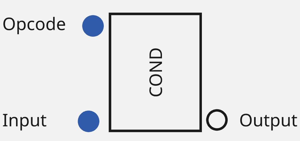
Plus a compact version again for our computer
17.1 Integrating the condition engine
Let’s add the condition engine to our computer to allow for conditional code execution! As we previously discussed, we take the instruction as a condition, the value from register 3. If we are then in condition mode AND the condition is satisfied, we forward the value to the program counter override.
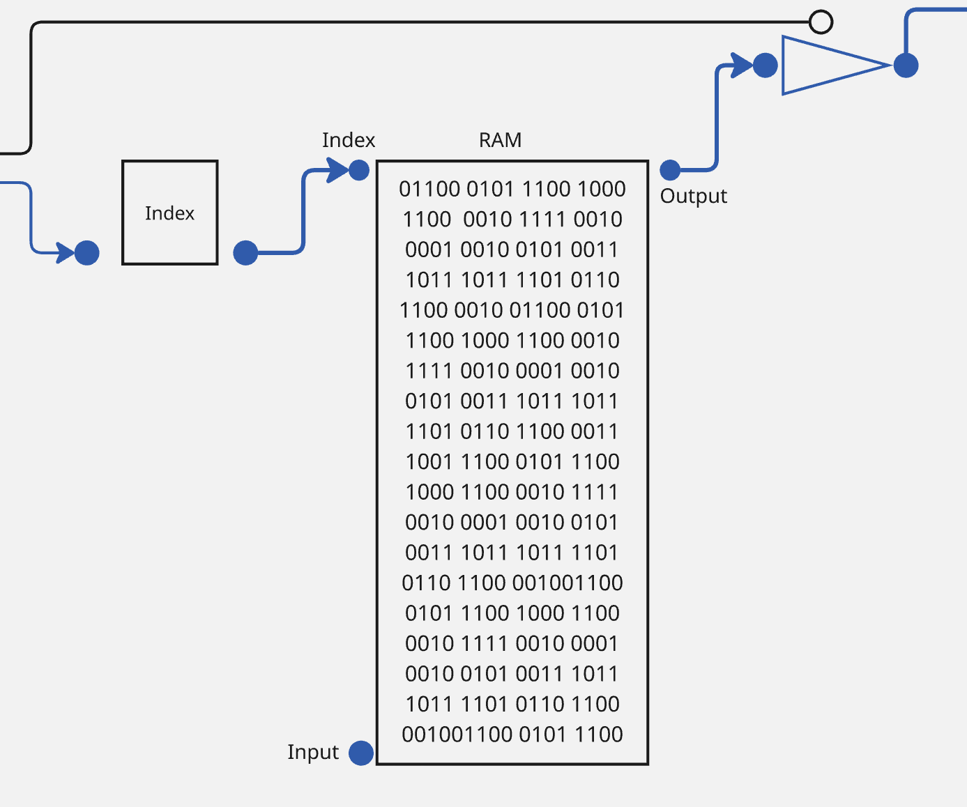
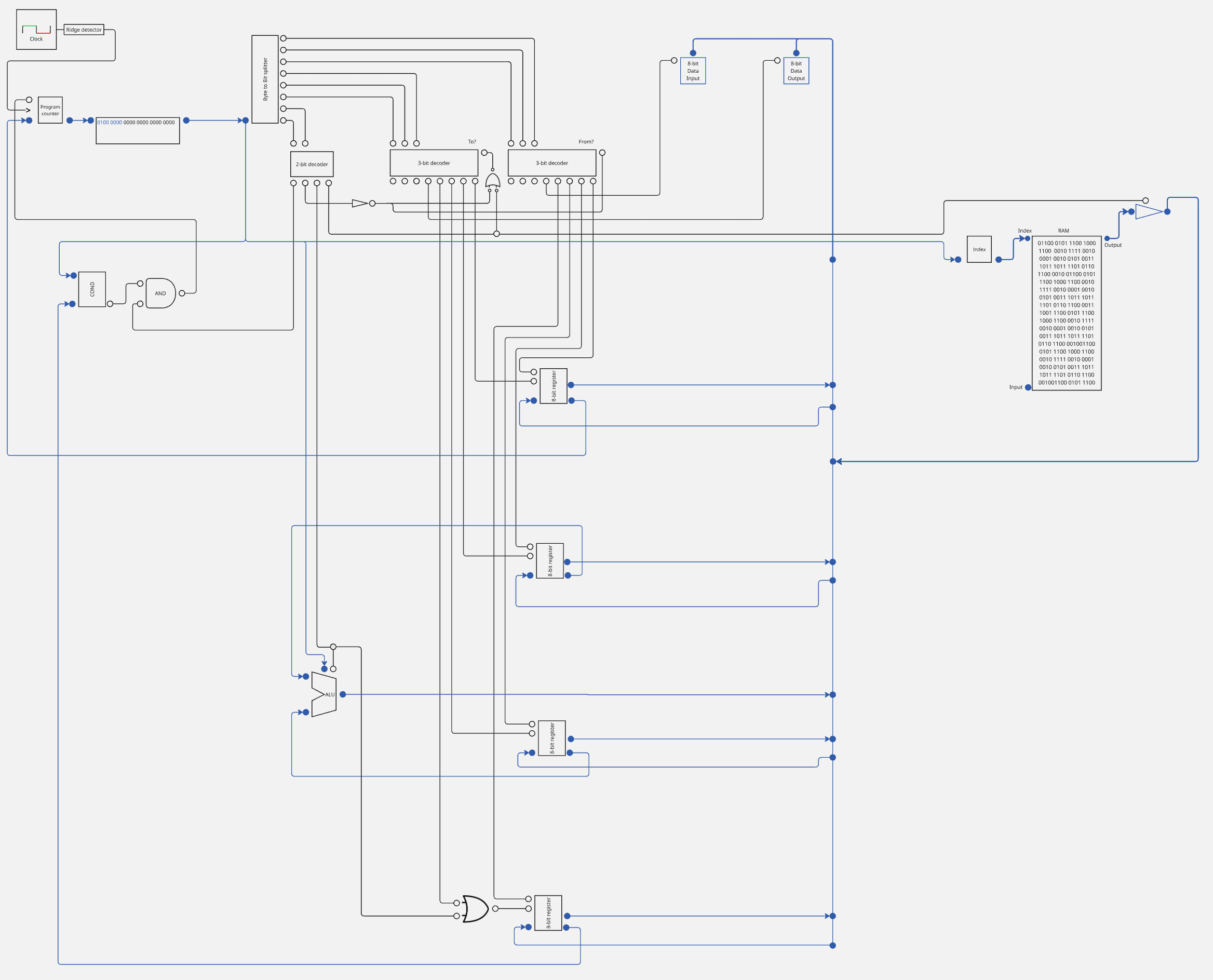
Goal 18: RAM
We still have a possible instruction left for which I have two ideas.
Idea nr. 1 is that we introduce a read operation from a specific memory location in RAM. That is, we could just tell the computer that we need to read from a specific address in RAM. RAM would then just be a large block of memory with an index that we can provide to get a specific address. We could then also provide where to load this into.
Which we could hook up like this, not forgetting to turn on the decoder for reading into the correct register:
With possible opcodes structured like this:
00
Load from RAM
01
Do some calculation.
10
Copy a value.
11
Condition
Just as with the copy instruction, we can use the existing logic for the register “save to?” selection, leaving us the three least significant bits to read the index in the RAM. Now, 2^3=8 addresses is really not much, but enough to give us an idea of what could be possible.
Annoyingly, we do not have enough bits to store a write to ram operation. But we can still reason what this would entail. We would need to turn the output of the register to read from on and then read from the common wire (i.e., the Bus). We then would need to enable write on the RAM and provide an index/ address to write to.
Goal 19: Immediate values
My second idea was that we use so-called immediate values with the opcode 00.
00
Immediate
01
Do some calculation.
10
Copy a value.
11
Condition
Since the opcode happens to be 00, the byte is preserved in the number it represents in the 6 least significant bits. We could just load this directly into a register - effectively saving us a few copy operations from the data input into the register we want.
For this, we need to pass the byte value directly to the bus and add an OR-gate to the load operation of a fixed register (e.g., Register 0).
Goal 20: CPU
We have finished the computer! We can now compute whatever we want, copy values, understand negative numbers, add them, subtract them, conditionally execute code based on data and pass values directly from the program into the register. To those missing multiplication and division in the circuit, don’t worry. We can represent these in our instruction as a series of repeated addition or subtraction. But you do have a point. We have not implemented everything you may expect. Modern CPUs have multiple registers, caches of decreasing size to operate faster on data that is likely needed, are able to predict branching and add additional, optimized circuits for common operations like multiplication, division, fused-multiply-add etc. There is much more to design and implement here. Depending on the use case of our computer, different components may be relevant.
Sources
Inside the Machine: An Illustrated Introduction to Microprocessors and Computer Architecture